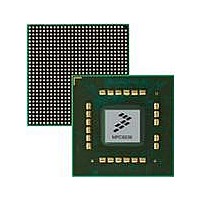
MPC8536DS Freescale Semiconductor, MPC8536DS Datasheet - Page 354

MPC8536DS
Manufacturer Part Number
MPC8536DS
Description
BOARD DEV SYSTEM MPC8536E
Manufacturer
Freescale Semiconductor
Series
PowerQUICC III™r
Type
MPUr
Datasheets
1.MPC8536EBVTAVLA.pdf
(127 pages)
2.MPC8536EBVTAVLA.pdf
(1706 pages)
3.MPC8536DS.pdf
(2 pages)
4.MPC8536DS.pdf
(126 pages)
Specifications of MPC8536DS
Contents
Board, Software and Documentation
Processor Series
MPC85xx
Core
e500
Data Bus Width
32 bit
Maximum Clock Frequency
667 MHz
Operating Supply Voltage
- 0.3 V to + 1.21 V
Maximum Operating Temperature
+ 105 C
Data Ram Size
32 KB
Interface Type
SPI, USB
Program Memory Type
DDR2, DDR3, SDRAM
Core Size
32 Bit
Program Memory Size
544KB
Cpu Speed
1.5GHz
Digital Ic Case Style
BGA
No. Of Pins
783
Supply Voltage Range
0.95V To 1.05V
Rohs Compliant
Yes
For Use With/related Products
MPC8536
Lead Free Status / RoHS Status
Lead free / RoHS Compliant
- MPC8536EBVTAVLA PDF datasheet
- MPC8536EBVTAVLA PDF datasheet #2
- MPC8536DS PDF datasheet #3
- MPC8536DS PDF datasheet #4
- Current page: 354 of 1706
- Download datasheet (15Mb)
DDR Memory Controller
The auto-refresh commands are staggered across the four possible banks to reduce the system’s
instantaneous power requirements. Three sets of auto refresh commands are issued on consecutive cycles
when the memory is fully populated with two DIMMs. The initial PRECHARGE-ALL commands are also
staggered in three groups for convenience. It is important to note that when entering self-refresh mode,
only one refresh command is issued simultaneously to all physical banks. For this entire refresh sequence,
no cycle optimization occurs for the usual case where fewer than four banks are installed. After the refresh
sequence completes, any pending memory request is initiated after an inactive period specified by
TIMING_CFG_1 [REFREC] and TIMING_CFG_3[EXT_REFREC]. In addition, posted refreshes are
supported to allow the refresh interval to be set to a larger value.
8.5.8.1
Refresh timing for the DDR SDRAM is controlled by the programmable timing parameter
TIMING_CFG_1 [REFREC], which specifies the number of memory bus clock cycles from the refresh
command until a logical bank activate command is allowed. The DDR memory controller implements
bank staggering for refreshes, as shown in
example).
System software is responsible for optimal configuration of TIMING_CFG_1 [REFREC] and
TIMING_CFG_3[EXT_REFREC] at reset. Configuration must be completed before DDR SDRAM
accesses are attempted.
8.5.8.2
In full-on mode, the DDR memory controller supplies the normal auto refresh to SDRAM. In sleep mode,
the DDR memory controller can be configured to take advantage of self-refreshing SDRAMs or to provide
no refresh support. Self-refresh support is enabled with the SREN memory control parameter.
8-80
SDRAM Clock
MCS[0,3]
MRAS
MCAS
DDR SDRAM Refresh Timing
MCS1
MCS2
DDR SDRAM Refresh and Power-Saving Modes
CKE
MA n
MPC8536E PowerQUICC III Integrated Processor Reference Manual, Rev. 1
Figure 8-56. DDR SDRAM Bank Staggered Auto Refresh Timing
0
1
2
3
Figure 8-56
4
5
6
(TIMING_CFG_1 [REFREC] = 10 in this
REFREC
7
8
9
10
11
0 or 3
Freescale Semiconductor
ROW
12
13
14
Related parts for MPC8536DS
Image
Part Number
Description
Manufacturer
Datasheet
Request
R
Part Number:
Description:
Manufacturer:
Freescale Semiconductor, Inc
Datasheet:
Part Number:
Description:
Manufacturer:
Freescale Semiconductor, Inc
Datasheet:
Part Number:
Description:
Manufacturer:
Freescale Semiconductor, Inc
Datasheet:
Part Number:
Description:
Manufacturer:
Freescale Semiconductor, Inc
Datasheet:
Part Number:
Description:
Manufacturer:
Freescale Semiconductor, Inc
Datasheet:
Part Number:
Description:
Manufacturer:
Freescale Semiconductor, Inc
Datasheet:
Part Number:
Description:
Manufacturer:
Freescale Semiconductor, Inc
Datasheet:
Part Number:
Description:
Manufacturer:
Freescale Semiconductor, Inc
Datasheet:
Part Number:
Description:
Manufacturer:
Freescale Semiconductor, Inc
Datasheet:
Part Number:
Description:
Manufacturer:
Freescale Semiconductor, Inc
Datasheet:
Part Number:
Description:
Manufacturer:
Freescale Semiconductor, Inc
Datasheet:
Part Number:
Description:
Manufacturer:
Freescale Semiconductor, Inc
Datasheet:
Part Number:
Description:
Manufacturer:
Freescale Semiconductor, Inc
Datasheet:
Part Number:
Description:
Manufacturer:
Freescale Semiconductor, Inc
Datasheet:
Part Number:
Description:
Manufacturer:
Freescale Semiconductor, Inc
Datasheet:


