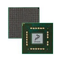
MPC8536DS Freescale Semiconductor, MPC8536DS Datasheet - Page 688

MPC8536DS
Manufacturer Part Number
MPC8536DS
Description
BOARD DEV SYSTEM MPC8536E
Manufacturer
Freescale Semiconductor
Series
PowerQUICC III™r
Type
MPUr
Datasheets
1.MPC8536EBVTAVLA.pdf
(127 pages)
2.MPC8536EBVTAVLA.pdf
(1706 pages)
3.MPC8536DS.pdf
(2 pages)
4.MPC8536DS.pdf
(126 pages)
Specifications of MPC8536DS
Contents
Board, Software and Documentation
Processor Series
MPC85xx
Core
e500
Data Bus Width
32 bit
Maximum Clock Frequency
667 MHz
Operating Supply Voltage
- 0.3 V to + 1.21 V
Maximum Operating Temperature
+ 105 C
Data Ram Size
32 KB
Interface Type
SPI, USB
Program Memory Type
DDR2, DDR3, SDRAM
Core Size
32 Bit
Program Memory Size
544KB
Cpu Speed
1.5GHz
Digital Ic Case Style
BGA
No. Of Pins
783
Supply Voltage Range
0.95V To 1.05V
Rohs Compliant
Yes
For Use With/related Products
MPC8536
Lead Free Status / RoHS Status
Lead free / RoHS Compliant
- MPC8536EBVTAVLA PDF datasheet
- MPC8536EBVTAVLA PDF datasheet #2
- MPC8536DS PDF datasheet #3
- MPC8536DS PDF datasheet #4
- Current page: 688 of 1706
- Download datasheet (15Mb)
Enhanced Local Bus Controller
13.4.1.4
The memory controller provides a data buffer control signal for the local bus (LBCTL). This signal is
activated when a GPCM-, FCM-, or UPM-controlled bank is accessed. LBCTL can be disabled by setting
ORn[BCTLD]. LBCTL can be further configured by LBCR[BCTLC] to act as an extra LWE or an extra
LOE signal when in GPCM mode.
If LBCTL is configured as a data buffer control (LBCR[BCTLC] = 00), the signal is asserted (high) on the
rising edge of the bus clock on the first cycle of the memory controller operation, coincident with LALE.
If the access is a write, LBCTL remains high for the whole duration. However, if the access is a read,
LBCTL is negated (low) with the negation of LALE so that the memory device is able to drive the bus. If
back-to-back read accesses are pending, LBCTL is asserted (high) one bus clock cycle before the next
transaction starts (that is, one bus clock cycle before LALE) to allow a whole bus cycle for the bus to turn
around before the next address is driven.
13.4.1.5
The eLBC supports the following kinds of atomic bus operations (set by BRn[ATOM]):
13-46
•
•
Read-after-write atomic (RAWA). When a write access hits a memory bank in which ATOM = 01,
the eLBC reserves the selected memory bank for the exclusive use of the accessing master.
While the bank is reserved, no other device can be granted access to this bank. The reservation is
released when the master that created it accesses the same bank with a read transaction. Additional
write transactions prior to the releasing read do not change reservation status, but are otherwise
processed normally. If the master fails to release the reservation within 256 bus clock cycles, the
reservation is released and an atomic error is reported (if enabled); additional write transactions
prior to the releasing read restart the reservation timer. This feature is intended for CAM
operations.
Write-after-read atomic (WARA). When a read access hits a memory bank in which ATOM = 10,
the eLBC reserves the bus for the exclusive use of the accessing master.
During the reservation period, no other device can be granted access to the atomic bank. The
reservation is released when the device that created it accesses the same bank with a write
transaction. Additional read transactions prior to the releasing write are otherwise processed
normally and do not change the reservation status. If the device fails to release the reservation
Data Buffer Control (LBCTL)
Atomic Operation
MPC8536E PowerQUICC III Integrated Processor Reference Manual, Rev. 1
Figure 13-31. Basic eLBC Bus Cycle with LALE, TA, and LCS n
LCLK
LCS n
LALE
LAD
TA
Address
Data
Freescale Semiconductor
Related parts for MPC8536DS
Image
Part Number
Description
Manufacturer
Datasheet
Request
R
Part Number:
Description:
Manufacturer:
Freescale Semiconductor, Inc
Datasheet:
Part Number:
Description:
Manufacturer:
Freescale Semiconductor, Inc
Datasheet:
Part Number:
Description:
Manufacturer:
Freescale Semiconductor, Inc
Datasheet:
Part Number:
Description:
Manufacturer:
Freescale Semiconductor, Inc
Datasheet:
Part Number:
Description:
Manufacturer:
Freescale Semiconductor, Inc
Datasheet:
Part Number:
Description:
Manufacturer:
Freescale Semiconductor, Inc
Datasheet:
Part Number:
Description:
Manufacturer:
Freescale Semiconductor, Inc
Datasheet:
Part Number:
Description:
Manufacturer:
Freescale Semiconductor, Inc
Datasheet:
Part Number:
Description:
Manufacturer:
Freescale Semiconductor, Inc
Datasheet:
Part Number:
Description:
Manufacturer:
Freescale Semiconductor, Inc
Datasheet:
Part Number:
Description:
Manufacturer:
Freescale Semiconductor, Inc
Datasheet:
Part Number:
Description:
Manufacturer:
Freescale Semiconductor, Inc
Datasheet:
Part Number:
Description:
Manufacturer:
Freescale Semiconductor, Inc
Datasheet:
Part Number:
Description:
Manufacturer:
Freescale Semiconductor, Inc
Datasheet:
Part Number:
Description:
Manufacturer:
Freescale Semiconductor, Inc
Datasheet:


