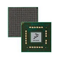
MPC8536DS Freescale Semiconductor, MPC8536DS Datasheet - Page 871

MPC8536DS
Manufacturer Part Number
MPC8536DS
Description
BOARD DEV SYSTEM MPC8536E
Manufacturer
Freescale Semiconductor
Series
PowerQUICC III™r
Type
MPUr
Datasheets
1.MPC8536EBVTAVLA.pdf
(127 pages)
2.MPC8536EBVTAVLA.pdf
(1706 pages)
3.MPC8536DS.pdf
(2 pages)
4.MPC8536DS.pdf
(126 pages)
Specifications of MPC8536DS
Contents
Board, Software and Documentation
Processor Series
MPC85xx
Core
e500
Data Bus Width
32 bit
Maximum Clock Frequency
667 MHz
Operating Supply Voltage
- 0.3 V to + 1.21 V
Maximum Operating Temperature
+ 105 C
Data Ram Size
32 KB
Interface Type
SPI, USB
Program Memory Type
DDR2, DDR3, SDRAM
Core Size
32 Bit
Program Memory Size
544KB
Cpu Speed
1.5GHz
Digital Ic Case Style
BGA
No. Of Pins
783
Supply Voltage Range
0.95V To 1.05V
Rohs Compliant
Yes
For Use With/related Products
MPC8536
Lead Free Status / RoHS Status
Lead free / RoHS Compliant
- MPC8536EBVTAVLA PDF datasheet
- MPC8536EBVTAVLA PDF datasheet #2
- MPC8536DS PDF datasheet #3
- MPC8536DS PDF datasheet #4
- Current page: 871 of 1706
- Download datasheet (15Mb)
Freescale Semiconductor
18–19
6–15
Bits
16
17
20
21
22
23
24
25
26
27
5
PERIOD
ESFDP
ESFDE
TCLK_
ETEP2
ETEP1
COPH
TMSR
Name
RTPE
PP2L
CIPH
FRD
—
—
MPC8536E PowerQUICC III Integrated Processor Reference Manual, Rev. 1
Table 14-114. TMR_CTRL Register Field Descriptions (continued)
Fiper2 pulse loopback mode enabled.
0 Trigger2 input is based upon normal external trigger input.
1 Fiper2 pulse is looped back into Trigger2 input.
1588 timer reference clock period. The timer clock counter will increment by TCLK_PERIOD every time
the accumulator register overflows. This clock period must be larger than the clock period of the timer
reference clock. For applications where user does not want the clock period to be added, they can
program this field to 1 to count the clock ticks. This field defaulted to 1 to count overflow ticks.
For nanosecond granularity on 1588 timer counter rate, the TCLK_PERIOD should be calculated using
the following equation:
Record Tx Time-Stamp to PAL Enable.
When set, and FCB[PTP] is set, the 8-byte time-stamp for the packet is written to the PAL located in
external memory location at an offset of 16 bytes from the start of the Data Buffer Pointer of the first
TxBD. For guidelines on using the RTPE bit, refer to
Transmit
FIPER Realignment Disable
0 Fiper Realignment is enabled.
1 Fiper Realignment is disabled.
Reserved
External Tx/Rx SFD Polarity.
0 Time stamp on rising edge of external SFD indication.
1 Time stamp on falling edge of external SFD indication.
External Tx/Rx SFD Enable.
0 Time stamp PTP TX frame based on MAC’s SFD indication.
1 Time stamp PTP TX frame based on external SFD indication from PHY.
External trigger 2 edge polarity
0 Time stamp on the rising edge of the external trigger
1 Time stamp on the falling edge of the external trigger
External trigger 1 edge polarity
0 time stamp on the rising edge of the external trigger
1 time stamp on the falling edge of the external trigger
Generated clock (TSEC_1588_CLK_OUT) output phase.
0 non-inverted divided clock is output
1 inverted divided clock is output
Oscillator input clock phase.
0 non-inverted timer input clock
1 inverted timer input clock (NOTE: this setting is reserved if CKSEL=01.)
Timer soft reset. When enabled, it resets all the timer registers and state machines.
0 normal operation
1 place entire timer in reset except control and config registers
NOTE: Prior to initiating timer reset (setting TMSR), must gracefully stop receiver (See
MACCFG1[RX_EN] description).
User programmable registers are not reset by the soft reset e.g. TMR_CTRL, TMR_TEMASK,
TMR_PEMASK, TMR_ADD, TMR_PRSC, TMROFF_H/L, TMR_ALARMn, and TMR_FIPERn.
Reserved
TCLK_PERIOD = 10
Packets.”
9
/Nominal_Frequency
Description
Section 14.6.7.5, “Time-Stamp Insertion on
Enhanced Three-Speed Ethernet Controllers
14-123
Related parts for MPC8536DS
Image
Part Number
Description
Manufacturer
Datasheet
Request
R
Part Number:
Description:
Manufacturer:
Freescale Semiconductor, Inc
Datasheet:
Part Number:
Description:
Manufacturer:
Freescale Semiconductor, Inc
Datasheet:
Part Number:
Description:
Manufacturer:
Freescale Semiconductor, Inc
Datasheet:
Part Number:
Description:
Manufacturer:
Freescale Semiconductor, Inc
Datasheet:
Part Number:
Description:
Manufacturer:
Freescale Semiconductor, Inc
Datasheet:
Part Number:
Description:
Manufacturer:
Freescale Semiconductor, Inc
Datasheet:
Part Number:
Description:
Manufacturer:
Freescale Semiconductor, Inc
Datasheet:
Part Number:
Description:
Manufacturer:
Freescale Semiconductor, Inc
Datasheet:
Part Number:
Description:
Manufacturer:
Freescale Semiconductor, Inc
Datasheet:
Part Number:
Description:
Manufacturer:
Freescale Semiconductor, Inc
Datasheet:
Part Number:
Description:
Manufacturer:
Freescale Semiconductor, Inc
Datasheet:
Part Number:
Description:
Manufacturer:
Freescale Semiconductor, Inc
Datasheet:
Part Number:
Description:
Manufacturer:
Freescale Semiconductor, Inc
Datasheet:
Part Number:
Description:
Manufacturer:
Freescale Semiconductor, Inc
Datasheet:
Part Number:
Description:
Manufacturer:
Freescale Semiconductor, Inc
Datasheet:


