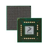
MPC8536DS Freescale Semiconductor, MPC8536DS Datasheet - Page 280

MPC8536DS
Manufacturer Part Number
MPC8536DS
Description
BOARD DEV SYSTEM MPC8536E
Manufacturer
Freescale Semiconductor
Series
PowerQUICC III™r
Type
MPUr
Datasheets
1.MPC8536EBVTAVLA.pdf
(127 pages)
2.MPC8536EBVTAVLA.pdf
(1706 pages)
3.MPC8536DS.pdf
(2 pages)
4.MPC8536DS.pdf
(126 pages)
Specifications of MPC8536DS
Contents
Board, Software and Documentation
Processor Series
MPC85xx
Core
e500
Data Bus Width
32 bit
Maximum Clock Frequency
667 MHz
Operating Supply Voltage
- 0.3 V to + 1.21 V
Maximum Operating Temperature
+ 105 C
Data Ram Size
32 KB
Interface Type
SPI, USB
Program Memory Type
DDR2, DDR3, SDRAM
Core Size
32 Bit
Program Memory Size
544KB
Cpu Speed
1.5GHz
Digital Ic Case Style
BGA
No. Of Pins
783
Supply Voltage Range
0.95V To 1.05V
Rohs Compliant
Yes
For Use With/related Products
MPC8536
Lead Free Status / RoHS Status
Lead free / RoHS Compliant
- MPC8536EBVTAVLA PDF datasheet
- MPC8536EBVTAVLA PDF datasheet #2
- MPC8536DS PDF datasheet #3
- MPC8536DS PDF datasheet #4
- Current page: 280 of 1706
- Download datasheet (15Mb)
DDR Memory Controller
8.3.2
The following sections describe the DDR SDRAM controller input and output signals, the meaning of their
different states, and relative timing information for assertion and negation.
8.3.2.1
Table 8-3
8-6
MDQS[0:8]/
MDQS[0:8]
MDQ[0:63]
Signal
describes the DDR controller memory interface signals.
Detailed Signal Descriptions
Memory Interface Signals
I/O
I/O Data bus. Both input and output signals on the DDR memory controller.
I/O Data strobes. Inputs with read data, outputs with write data.
O
O
I
I
MPC8536E PowerQUICC III Integrated Processor Reference Manual, Rev. 1
Table 8-3. Memory Interface Signals—Detailed Signal Descriptions
As outputs, the data strobes are driven by the DDR memory controller during a write transaction. The
memory controller always drives these signals low unless a read has been issued and incoming data
strobes are expected. This keeps the data strobes from floating high when there are no transactions on
the DRAM interface.
As inputs, the data strobes are driven by the external DDR SDRAMs during a read transaction. The data
strobes are used by the memory controller to synchronize data latching.
As outputs for the bidirectional data bus, these signals operate as described below.
As inputs for the bidirectional data bus, these signals operate as described below.
Meaning
Meaning
Meaning
Meaning
Timing Assertion/Negation—Driven coincident with corresponding data strobes (MDQS) signal.
Timing Assertion/Negation—The DDR SDRAM drives data during a READ transaction.
Timing Assertion/Negation—If a WRITE command is registered at clock edge n , data strobes at the
Timing Assertion/Negation—If a READ command is registered at clock edge n , and the latency is
State
State
State
State
Asserted/Negated—Represent the value of data being driven by the DDR memory controller.
High impedance—No READ or WRITE command is in progress; data is not being driven by
Asserted/Negated—Represents the state of data being driven by the external DDR
High impedance—No READ or WRITE command in progress; data is not being driven by the
Asserted/Negated—Driven high when positive capture data is transmitted and driven low
Asserted/Negated—Driven high when positive capture data is received and driven low when
the memory controller or the DRAM.
SDRAMs.
memory controller or the DRAM.
when negative capture data is transmitted. Centered in the data “eye” for writes;
coincident with the data eye for reads. Treated as a clock. Data is valid when signals
toggle. See
DRAM assert centered in the data eye on clock edge n + 1. See the JEDEC DDR
SDRAM specification for more information.
negative capture data is received. Centered in the data eye for writes; coincident with
the data eye for reads. Treated as a clock. Data is valid when signals toggle. See
Table 8-50
programmed in TIMING_CFG_1[CASLAT] to be m clocks, data strobes at the DRAM
assert coincident with the data on clock edge n + m . See the JEDEC DDR SDRAM
specification for more information.
for byte lane assignments.
Table 8-50
for byte lane assignments.
Description
Freescale Semiconductor
Related parts for MPC8536DS
Image
Part Number
Description
Manufacturer
Datasheet
Request
R
Part Number:
Description:
Manufacturer:
Freescale Semiconductor, Inc
Datasheet:
Part Number:
Description:
Manufacturer:
Freescale Semiconductor, Inc
Datasheet:
Part Number:
Description:
Manufacturer:
Freescale Semiconductor, Inc
Datasheet:
Part Number:
Description:
Manufacturer:
Freescale Semiconductor, Inc
Datasheet:
Part Number:
Description:
Manufacturer:
Freescale Semiconductor, Inc
Datasheet:
Part Number:
Description:
Manufacturer:
Freescale Semiconductor, Inc
Datasheet:
Part Number:
Description:
Manufacturer:
Freescale Semiconductor, Inc
Datasheet:
Part Number:
Description:
Manufacturer:
Freescale Semiconductor, Inc
Datasheet:
Part Number:
Description:
Manufacturer:
Freescale Semiconductor, Inc
Datasheet:
Part Number:
Description:
Manufacturer:
Freescale Semiconductor, Inc
Datasheet:
Part Number:
Description:
Manufacturer:
Freescale Semiconductor, Inc
Datasheet:
Part Number:
Description:
Manufacturer:
Freescale Semiconductor, Inc
Datasheet:
Part Number:
Description:
Manufacturer:
Freescale Semiconductor, Inc
Datasheet:
Part Number:
Description:
Manufacturer:
Freescale Semiconductor, Inc
Datasheet:
Part Number:
Description:
Manufacturer:
Freescale Semiconductor, Inc
Datasheet:


