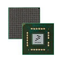
MPC8536DS Freescale Semiconductor, MPC8536DS Datasheet - Page 678

MPC8536DS
Manufacturer Part Number
MPC8536DS
Description
BOARD DEV SYSTEM MPC8536E
Manufacturer
Freescale Semiconductor
Series
PowerQUICC III™r
Type
MPUr
Datasheets
1.MPC8536EBVTAVLA.pdf
(127 pages)
2.MPC8536EBVTAVLA.pdf
(1706 pages)
3.MPC8536DS.pdf
(2 pages)
4.MPC8536DS.pdf
(126 pages)
Specifications of MPC8536DS
Contents
Board, Software and Documentation
Processor Series
MPC85xx
Core
e500
Data Bus Width
32 bit
Maximum Clock Frequency
667 MHz
Operating Supply Voltage
- 0.3 V to + 1.21 V
Maximum Operating Temperature
+ 105 C
Data Ram Size
32 KB
Interface Type
SPI, USB
Program Memory Type
DDR2, DDR3, SDRAM
Core Size
32 Bit
Program Memory Size
544KB
Cpu Speed
1.5GHz
Digital Ic Case Style
BGA
No. Of Pins
783
Supply Voltage Range
0.95V To 1.05V
Rohs Compliant
Yes
For Use With/related Products
MPC8536
Lead Free Status / RoHS Status
Lead free / RoHS Compliant
- MPC8536EBVTAVLA PDF datasheet
- MPC8536EBVTAVLA PDF datasheet #2
- MPC8536DS PDF datasheet #3
- MPC8536DS PDF datasheet #4
- Current page: 678 of 1706
- Download datasheet (15Mb)
Enhanced Local Bus Controller
Table 13-24
13-36
16–19 CWTO Command wait time-out. For FCM commands that wait on LFRB being sampled high (CW0, CW1,
21–22
24–25
0–15
Bits
20
23
ECCM ECC mode. When hardware checking and/or generation of error correcting codes (ECC) is enabled
Name
BOOT Flash auto-boot load mode. During system boot from NAND Flash EEPROM, this bit remains set to
describes FMR fields.
—
—
—
Reserved
RBW and RSW), FCM pauses execution of the instruction sequence until either LFRB is sampled high,
or a timer controlled by CTO expires, whichever occurs first. The time-out in the latter case is:
0000 256 cycles of LCLK
0001 512 cycles of LCLK
0010 1024 cycles of LCLK
0011 2048 cycles of LCLK
0100 4096 cycles of LCLK
0101 8192 cycles of LCLK
0110 16,384 cycles of LCLK
0111 32,768 cycles of LCLK
1000 65,536 cycles of LCLK
1001 131,072 cycles of LCLK
1010 262,144 cycles of LCLK
1011 524,288 cycles of LCLK
1100 1,048,576 cycles of LCLK
1101 2,097,152 cycles of LCLK
1110 4,194,304 cycles of LCLK
1111 8,388,608 cycles of LCLK
alter the use of the FCM buffer RAM. Software should clear BOOT once FCM is to be restored to
normal operation. Setting BOOT without auto-boot in progress only alters the mapping of the buffer
RAM.
0 FCM is operating in normal functional mode, with an 8 Kbyte FCM buffer RAM.
1 eLBC has been configured—either from reset or by a special operation OP = 01—to auto-load a
Reserved
(that is, when BR n [DECC] is 01 or 10, and full page transfers are specified with FBCR[BC] = 0), ECCM
sets the ECC block size and position of the ECC code word(s) in the NAND Flash spare region for both
checking and generation functions. The format of the ECC code word conforms with the
Samsung/Toshiba spare region assignment specifications.
0 ECC is checked/calculated over 512-Byte blocks. A 24-bit ECC is assigned to spare region bytes at
1 ECC is checked/calculated over 512-Byte blocks. A 24-bit ECC is assigned to spare region bytes at
Reserved
MPC8536E PowerQUICC III Integrated Processor Reference Manual, Rev. 1
4-Kbyte boot block into the FCM buffer RAM, which maps only the 4 Kbytes of NAND flash main
data region comprising the boot block. Any access to the buffer RAM is delayed until the entire boot
block has been loaded.
offsets ( N ×16)+6 through ( N ×16)+8 for spare region N , N = 0–3.
offsets ( N ×16)+8 through ( N ×16)+10 for spare region N , N = 0–3.
Table 13-24. FMR Field Descriptions
Description
Freescale Semiconductor
Related parts for MPC8536DS
Image
Part Number
Description
Manufacturer
Datasheet
Request
R
Part Number:
Description:
Manufacturer:
Freescale Semiconductor, Inc
Datasheet:
Part Number:
Description:
Manufacturer:
Freescale Semiconductor, Inc
Datasheet:
Part Number:
Description:
Manufacturer:
Freescale Semiconductor, Inc
Datasheet:
Part Number:
Description:
Manufacturer:
Freescale Semiconductor, Inc
Datasheet:
Part Number:
Description:
Manufacturer:
Freescale Semiconductor, Inc
Datasheet:
Part Number:
Description:
Manufacturer:
Freescale Semiconductor, Inc
Datasheet:
Part Number:
Description:
Manufacturer:
Freescale Semiconductor, Inc
Datasheet:
Part Number:
Description:
Manufacturer:
Freescale Semiconductor, Inc
Datasheet:
Part Number:
Description:
Manufacturer:
Freescale Semiconductor, Inc
Datasheet:
Part Number:
Description:
Manufacturer:
Freescale Semiconductor, Inc
Datasheet:
Part Number:
Description:
Manufacturer:
Freescale Semiconductor, Inc
Datasheet:
Part Number:
Description:
Manufacturer:
Freescale Semiconductor, Inc
Datasheet:
Part Number:
Description:
Manufacturer:
Freescale Semiconductor, Inc
Datasheet:
Part Number:
Description:
Manufacturer:
Freescale Semiconductor, Inc
Datasheet:
Part Number:
Description:
Manufacturer:
Freescale Semiconductor, Inc
Datasheet:


