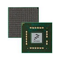
MPC8536DS Freescale Semiconductor, MPC8536DS Datasheet - Page 235

MPC8536DS
Manufacturer Part Number
MPC8536DS
Description
BOARD DEV SYSTEM MPC8536E
Manufacturer
Freescale Semiconductor
Series
PowerQUICC III™r
Type
MPUr
Datasheets
1.MPC8536EBVTAVLA.pdf
(127 pages)
2.MPC8536EBVTAVLA.pdf
(1706 pages)
3.MPC8536DS.pdf
(2 pages)
4.MPC8536DS.pdf
(126 pages)
Specifications of MPC8536DS
Contents
Board, Software and Documentation
Processor Series
MPC85xx
Core
e500
Data Bus Width
32 bit
Maximum Clock Frequency
667 MHz
Operating Supply Voltage
- 0.3 V to + 1.21 V
Maximum Operating Temperature
+ 105 C
Data Ram Size
32 KB
Interface Type
SPI, USB
Program Memory Type
DDR2, DDR3, SDRAM
Core Size
32 Bit
Program Memory Size
544KB
Cpu Speed
1.5GHz
Digital Ic Case Style
BGA
No. Of Pins
783
Supply Voltage Range
0.95V To 1.05V
Rohs Compliant
Yes
For Use With/related Products
MPC8536
Lead Free Status / RoHS Status
Lead free / RoHS Compliant
- MPC8536EBVTAVLA PDF datasheet
- MPC8536EBVTAVLA PDF datasheet #2
- MPC8536DS PDF datasheet #3
- MPC8536DS PDF datasheet #4
- Current page: 235 of 1706
- Download datasheet (15Mb)
The L2CEWCRn registers contain identical fields, which are described in
6.3.1.3
The registers described in this section, the L2 memory-mapped SRAM base address registers 0–1
(L2SRBARn) and the L2 memory-mapped SRAM base address registers extended address 0–1
(L2SRBAREAn), control the memory-mapped SRAM mode functionality. Together, these two pairs of
registers define memory blocks that can be mapped into the L2 cache.
Specified SRAM base addresses must be aligned to the size of the SRAM region. If L2CTL[L2SRAM]
specifies one memory-mapped SRAM block, its base address must be written to the pair L2SRBAR0 and
L2SRBAREA0; if it specifies two memory-mapped SRAM blocks, L2SRBAR0 and L2SRBAREA0 are
used for the first SRAM block and L2SRBAR1 and L2SRBAREA1 are used for the second block.
Freescale Semiconductor
4–31 SIZMASK
Bits
2–3
0
1
Name
LOCK
—
E
L2 Memory-Mapped SRAM Registers
External write enable. An external write matching the address window defined by
L2CEWAR n /L2CEWAREA n /L2CEWCR n is allocated or updated in the L2 cache.
0 External writes for the L2CEWAR n /L2CEWAREA n /L2CEWCR n set are disabled.
1 External writes are enabled for the L2CEWAR n /L2CEWAREA n /L2CEWCR n set.
Lock lines in the targeted cache. An external write matching the address window defined by
L2CEWAR n /L2CEWAREA n /L2CEWCR n is locked in the L2 cache when it is allocated or updated.
0 The locked bit is not set when a line is allocated unless explicitly specified by transaction attributes.
1 Cache lines are allocated as locked. A hit to a valid, unlocked line sets the lock.
Reserved
Mask size. Defines the size of the naturally aligned address region for cache external writes. The
address region must be aligned to a boundary that is a multiple of the mask size. Any value not listed
below is illegal and produces boundedly undefined results.
1111 1111 1111 1111 1111 1111 1111 256 bytes
1111 1111 1111 1111 1111 1111 1110 512 bytes
1111 1111 1111 1111 1111 1111 1100 1 Kbyte
1111 1111 1111 1111 1111 1111 1000 2 Kbytes
1111 1111 1111 1111 1111 1111 0000 4 Kbytes
1111 1111 1111 1111 1111 1110 0000 8 Kbytes
1111 1111 1111 1111 1111 1100 0000 16 Kbytes
1111 1111 1111 1111 1111 1000 0000 32 Kbytes
1111 1111 1111 1111 1111 0000 0000 64 Kbytes
1111 1111 1111 1111 1110 0000 0000 128 Kbytes
1111 1111 1111 1111 1100 0000 0000 256 Kbytes
1111 1111 1111 1111 1000 0000 0000 512 Kbytes
1111 1111 1111 1111 0000 0000 0000 1 Mbyte
1111 1111 1111 1110 0000 0000 0000 2 Mbytes
1111 1111 1111 1100 0000 0000 0000 4 Mbytes
MPC8536E PowerQUICC III Integrated Processor Reference Manual, Rev. 1
Table 6-7. L2CEWCR n Field Descriptions
Description
1111 1111 1111 1000 0000 0000 0000 8 Mbytes
1111 1111 1111 0000 0000 0000 0000 16 Mbytes
1111 1111 1110 0000 0000 0000 0000 32 Mbytes
1111 1111 1100 0000 0000 0000 0000 64 Mbytes
1111 1111 1000 0000 0000 0000 0000 128 Mbytes
1111 1111 0000 0000 0000 0000 0000 256 Mbytes
1111 1110 0000 0000 0000 0000 0000 512 Mbytes
1111 1100 0000 0000 0000 0000 0000 1 Gbyte
1111 1000 0000 0000 0000 0000 0000 2 Gbytes
1111 0000 0000 0000 0000 0000 0000 4 Gbytes
1110 0000 0000 0000 0000 0000 0000 8 Gbytes
1100 0000 0000 0000 0000 0000 0000 16 Gbytes
1000 0000 0000 0000 0000 0000 0000 32 Gbytes
0000 0000 0000 0000 0000 0000 0000 64 Gbytes
Table
6-7.
L2 Look-Aside Cache/SRAM
6-15
Related parts for MPC8536DS
Image
Part Number
Description
Manufacturer
Datasheet
Request
R
Part Number:
Description:
Manufacturer:
Freescale Semiconductor, Inc
Datasheet:
Part Number:
Description:
Manufacturer:
Freescale Semiconductor, Inc
Datasheet:
Part Number:
Description:
Manufacturer:
Freescale Semiconductor, Inc
Datasheet:
Part Number:
Description:
Manufacturer:
Freescale Semiconductor, Inc
Datasheet:
Part Number:
Description:
Manufacturer:
Freescale Semiconductor, Inc
Datasheet:
Part Number:
Description:
Manufacturer:
Freescale Semiconductor, Inc
Datasheet:
Part Number:
Description:
Manufacturer:
Freescale Semiconductor, Inc
Datasheet:
Part Number:
Description:
Manufacturer:
Freescale Semiconductor, Inc
Datasheet:
Part Number:
Description:
Manufacturer:
Freescale Semiconductor, Inc
Datasheet:
Part Number:
Description:
Manufacturer:
Freescale Semiconductor, Inc
Datasheet:
Part Number:
Description:
Manufacturer:
Freescale Semiconductor, Inc
Datasheet:
Part Number:
Description:
Manufacturer:
Freescale Semiconductor, Inc
Datasheet:
Part Number:
Description:
Manufacturer:
Freescale Semiconductor, Inc
Datasheet:
Part Number:
Description:
Manufacturer:
Freescale Semiconductor, Inc
Datasheet:
Part Number:
Description:
Manufacturer:
Freescale Semiconductor, Inc
Datasheet:


