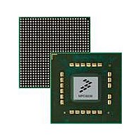
MPC8536DS Freescale Semiconductor, MPC8536DS Datasheet - Page 716

MPC8536DS
Manufacturer Part Number
MPC8536DS
Description
BOARD DEV SYSTEM MPC8536E
Manufacturer
Freescale Semiconductor
Series
PowerQUICC III™r
Type
MPUr
Datasheets
1.MPC8536EBVTAVLA.pdf
(127 pages)
2.MPC8536EBVTAVLA.pdf
(1706 pages)
3.MPC8536DS.pdf
(2 pages)
4.MPC8536DS.pdf
(126 pages)
Specifications of MPC8536DS
Contents
Board, Software and Documentation
Processor Series
MPC85xx
Core
e500
Data Bus Width
32 bit
Maximum Clock Frequency
667 MHz
Operating Supply Voltage
- 0.3 V to + 1.21 V
Maximum Operating Temperature
+ 105 C
Data Ram Size
32 KB
Interface Type
SPI, USB
Program Memory Type
DDR2, DDR3, SDRAM
Core Size
32 Bit
Program Memory Size
544KB
Cpu Speed
1.5GHz
Digital Ic Case Style
BGA
No. Of Pins
783
Supply Voltage Range
0.95V To 1.05V
Rohs Compliant
Yes
For Use With/related Products
MPC8536
Lead Free Status / RoHS Status
Lead free / RoHS Compliant
- MPC8536EBVTAVLA PDF datasheet
- MPC8536EBVTAVLA PDF datasheet #2
- MPC8536DS PDF datasheet #3
- MPC8536DS PDF datasheet #4
- Current page: 716 of 1706
- Download datasheet (15Mb)
Enhanced Local Bus Controller
13.4.4
UPMs are flexible interfaces that connect to a wide range of memory devices. At the heart of each UPM
is an internal RAM array that specifies the logical value driven on the external memory control signals
(LCSn, LBS[0:3] and LGPL[0:5]) for a given clock cycle. Each word in the RAM array provides bits that
allow a memory access to be controlled with a resolution of up to one quarter of the external bus clock
period on the byte-select and chip-select lines. A gap of 2 dead LCLK cycles is present on the UPM
interface between UPM transactions.
13-74
3. FCM reads the spare regions of the first two pages of the current block, checking the bad block
4. The FCM optionally performs ECC checking at boot time depending on the configuration selected
5. FCM performs a sequence of random-access page reads, reading entire pages from the boot block
6. The CPU now commences fetching instructions, in random order, from the FCM buffer RAM. This
indication (BI) bytes to validate the block for reading. BI bytes must all hold the value 0xFF for
the page to be considered readable.
— For small-page devices, BI is a single byte read from spare region byte offset 5.
— For large-page devices, BI is a single byte read from spare region byte offset 0.
If either of the first two pages of the current block are marked invalid, then the boot block index is
incremented by 1, and FCM repeats step 3. eLBC will continue searching for a bootable block
indefinitely, therefore at least one block must be marked valid for boot loading to proceed. At the
conclusion of the boot block search, the value of FBAR[BLK] points to the boot block.
during reset. If ECC checking is enabled, the FCM recovers from the spare region the stored ECC
for each 512-byte block of boot data. The boot block must be prepared with ECC protection.
During ECC generation, software should use FMR[ECCM] = 0 for small-page devices, and
FMR[ECCM] = 1 for large-page devices.
until 4 Kbytes have been saved to the FCM buffer RAM. If ECC checking is enabled, the ECC of
each 512-byte region is verified and single-bit errors are corrected if possible. If FCM is unable to
correct ECC errors, eLBC halts the boot process and signals an unrecoverable error by asserting
the hreset_req signal.
first-level boot loader typically copies a secondary boot loader into system memory, and continues
booting from there. Boot software must clear FMR[BOOT] to enable normal operation of FCM.
User-Programmable Machines (UPMs)
If the LGPL4/LGTA/LFRB/LUPWAIT/LPBSE signal is used as both an
input and an output, a weak pull-up is required. Refer to the hardware
specification for details regarding termination options.
MPC8536E PowerQUICC III Integrated Processor Reference Manual, Rev. 1
NOTE
Freescale Semiconductor
Related parts for MPC8536DS
Image
Part Number
Description
Manufacturer
Datasheet
Request
R
Part Number:
Description:
Manufacturer:
Freescale Semiconductor, Inc
Datasheet:
Part Number:
Description:
Manufacturer:
Freescale Semiconductor, Inc
Datasheet:
Part Number:
Description:
Manufacturer:
Freescale Semiconductor, Inc
Datasheet:
Part Number:
Description:
Manufacturer:
Freescale Semiconductor, Inc
Datasheet:
Part Number:
Description:
Manufacturer:
Freescale Semiconductor, Inc
Datasheet:
Part Number:
Description:
Manufacturer:
Freescale Semiconductor, Inc
Datasheet:
Part Number:
Description:
Manufacturer:
Freescale Semiconductor, Inc
Datasheet:
Part Number:
Description:
Manufacturer:
Freescale Semiconductor, Inc
Datasheet:
Part Number:
Description:
Manufacturer:
Freescale Semiconductor, Inc
Datasheet:
Part Number:
Description:
Manufacturer:
Freescale Semiconductor, Inc
Datasheet:
Part Number:
Description:
Manufacturer:
Freescale Semiconductor, Inc
Datasheet:
Part Number:
Description:
Manufacturer:
Freescale Semiconductor, Inc
Datasheet:
Part Number:
Description:
Manufacturer:
Freescale Semiconductor, Inc
Datasheet:
Part Number:
Description:
Manufacturer:
Freescale Semiconductor, Inc
Datasheet:
Part Number:
Description:
Manufacturer:
Freescale Semiconductor, Inc
Datasheet:


