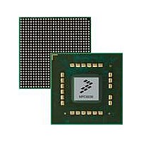
MPC8536DS Freescale Semiconductor, MPC8536DS Datasheet - Page 604

MPC8536DS
Manufacturer Part Number
MPC8536DS
Description
BOARD DEV SYSTEM MPC8536E
Manufacturer
Freescale Semiconductor
Series
PowerQUICC III™r
Type
MPUr
Datasheets
1.MPC8536EBVTAVLA.pdf
(127 pages)
2.MPC8536EBVTAVLA.pdf
(1706 pages)
3.MPC8536DS.pdf
(2 pages)
4.MPC8536DS.pdf
(126 pages)
Specifications of MPC8536DS
Contents
Board, Software and Documentation
Processor Series
MPC85xx
Core
e500
Data Bus Width
32 bit
Maximum Clock Frequency
667 MHz
Operating Supply Voltage
- 0.3 V to + 1.21 V
Maximum Operating Temperature
+ 105 C
Data Ram Size
32 KB
Interface Type
SPI, USB
Program Memory Type
DDR2, DDR3, SDRAM
Core Size
32 Bit
Program Memory Size
544KB
Cpu Speed
1.5GHz
Digital Ic Case Style
BGA
No. Of Pins
783
Supply Voltage Range
0.95V To 1.05V
Rohs Compliant
Yes
For Use With/related Products
MPC8536
Lead Free Status / RoHS Status
Lead free / RoHS Compliant
- MPC8536EBVTAVLA PDF datasheet
- MPC8536EBVTAVLA PDF datasheet #2
- MPC8536DS PDF datasheet #3
- MPC8536DS PDF datasheet #4
- Current page: 604 of 1706
- Download datasheet (15Mb)
I
Figure 11-8
address components of the I
11.4.1.1
When the I
by sending a START condition. As shown in
transition of SDA while SCL is high. This condition denotes the beginning of a new data transfer. Each
data transfer can contain several bytes and awakens all slaves. The START condition is initiated by a
software write that sets I2CCR[MSTA].
11.4.1.2
The first byte of data is transferred by the master immediately after the START condition is the slave
address. This is a seven-bit calling address followed by a R/W bit, which indicates the direction of the data
being transferred to the slave. Each slave in the system has a unique address. In addition, when the I
module is operating as a master, it must not transmit an address that is the same as its slave address. An
I
undefined.
Only the slave with a calling address that matches the one transmitted by the master responds by returning
an acknowledge bit (pulling the SDA signal low at the 9th clock) as shown in
acknowledges the address, the master should generate a STOP condition or a repeated START condition.
When slave addressing is successful (and SCL returns to zero), the data transfer can proceed on a byte-to-byte
basis in the direction specified by the R/W bit sent by the calling master.
11-12
2
2
C Interfaces
C device cannot be master and slave at the same time; if this is attempted, the results are boundedly
SDA
SDA
SCL
SCL
START
START
2
C bus is not engaged (both SDA and SCL lines are at logic high), a master can initiate a transfer
shows the interaction of these four parts with the calling address, data byte, and new calling
START Condition
Slave Address Transmission
A0 A1 A2 A3 A4 A5 A6 R/W
A0 A1 A2 A3 A4 A5 A6 R/W
1
1
2
MPC8536E PowerQUICC III Integrated Processor Reference Manual, Rev. 1
2
Calling address
Calling address
3
3
2
4
4
C protocol. The details of the protocol are described in the following sections.
Figure 11-8. I
5
5
6
6
7
7
Read/
write
Read/
write
2
C Interface Transaction Protocol
8
8
Figure
Ack
Ack
9
9
XX
11-8, a START condition is defined as a high-to-low
Repeated
START
XX
A0 A1 A2 A3 A4 A5 A6 R/W
D0 D1 D2 D3 D4 D5 D6 D7
1
1
2
2
New calling address
3
3
Data byte
4
4
5
5
Figure
6
6
7
7
Freescale Semiconductor
11-8. If no slave
8
8
No
ack
No
ack
9
9
STOP
STOP
2
C
Related parts for MPC8536DS
Image
Part Number
Description
Manufacturer
Datasheet
Request
R
Part Number:
Description:
Manufacturer:
Freescale Semiconductor, Inc
Datasheet:
Part Number:
Description:
Manufacturer:
Freescale Semiconductor, Inc
Datasheet:
Part Number:
Description:
Manufacturer:
Freescale Semiconductor, Inc
Datasheet:
Part Number:
Description:
Manufacturer:
Freescale Semiconductor, Inc
Datasheet:
Part Number:
Description:
Manufacturer:
Freescale Semiconductor, Inc
Datasheet:
Part Number:
Description:
Manufacturer:
Freescale Semiconductor, Inc
Datasheet:
Part Number:
Description:
Manufacturer:
Freescale Semiconductor, Inc
Datasheet:
Part Number:
Description:
Manufacturer:
Freescale Semiconductor, Inc
Datasheet:
Part Number:
Description:
Manufacturer:
Freescale Semiconductor, Inc
Datasheet:
Part Number:
Description:
Manufacturer:
Freescale Semiconductor, Inc
Datasheet:
Part Number:
Description:
Manufacturer:
Freescale Semiconductor, Inc
Datasheet:
Part Number:
Description:
Manufacturer:
Freescale Semiconductor, Inc
Datasheet:
Part Number:
Description:
Manufacturer:
Freescale Semiconductor, Inc
Datasheet:
Part Number:
Description:
Manufacturer:
Freescale Semiconductor, Inc
Datasheet:
Part Number:
Description:
Manufacturer:
Freescale Semiconductor, Inc
Datasheet:


