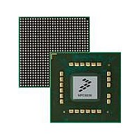
MPC8536DS Freescale Semiconductor, MPC8536DS Datasheet - Page 704

MPC8536DS
Manufacturer Part Number
MPC8536DS
Description
BOARD DEV SYSTEM MPC8536E
Manufacturer
Freescale Semiconductor
Series
PowerQUICC III™r
Type
MPUr
Datasheets
1.MPC8536EBVTAVLA.pdf
(127 pages)
2.MPC8536EBVTAVLA.pdf
(1706 pages)
3.MPC8536DS.pdf
(2 pages)
4.MPC8536DS.pdf
(126 pages)
Specifications of MPC8536DS
Contents
Board, Software and Documentation
Processor Series
MPC85xx
Core
e500
Data Bus Width
32 bit
Maximum Clock Frequency
667 MHz
Operating Supply Voltage
- 0.3 V to + 1.21 V
Maximum Operating Temperature
+ 105 C
Data Ram Size
32 KB
Interface Type
SPI, USB
Program Memory Type
DDR2, DDR3, SDRAM
Core Size
32 Bit
Program Memory Size
544KB
Cpu Speed
1.5GHz
Digital Ic Case Style
BGA
No. Of Pins
783
Supply Voltage Range
0.95V To 1.05V
Rohs Compliant
Yes
For Use With/related Products
MPC8536
Lead Free Status / RoHS Status
Lead free / RoHS Compliant
- MPC8536EBVTAVLA PDF datasheet
- MPC8536EBVTAVLA PDF datasheet #2
- MPC8536DS PDF datasheet #3
- MPC8536DS PDF datasheet #4
- Current page: 704 of 1706
- Download datasheet (15Mb)
Enhanced Local Bus Controller
512 bytes appear as main region data, and 16 bytes appear as spare region data. The EEPROM’s page
numbered P is associated with buffer number (P mod 8), where P = FPAR[PI]. Since the bank size set by
ORn[AM] will be greater than 8 Kbytes, an identical image of the FCM buffer RAM appears replicated
every 8 Kbytes throughout the bank address space. It is recommended that the bank size be set to 32
Kbytes, which covers a single NAND Flash block for small-page devices.
For FCM commands, register FPAR sets the page address and, therefore, also the buffer number.In the case
that FBCR[BC] = 0, FCM transfers an entire page, comprising the 512-byte main region followed by the
16-byte spare region; the 496-byte reserved region is not accessed, and remains undefined for software.
However, for commands given a specific byte count in FBCR[BC], FPAR[MS] locates the starting address
in either the main region (MS = 0) or the spare region (MS = 1). Where different eLBC banks control both
small and large-page devices, a large-page 4-Kbyte buffer must be assigned to either the first 4 or last 4
small-page buffers.
13.4.3.1.2
The FCM buffer space is divided into two 4 Kbyte buffers for large-page devices (ORn[PGS] = 1), mapped
as shown in
appear as main region data, and 64 bytes appear as spare region data. The EEPROM’s page numbered P
is associated with buffer number (P mod 2), where P = FPAR[PI]. Since the bank size set by ORn[AM]
will be greater than 8 Kbytes, an identical image of the FCM buffer RAM appears replicated every 8
Kbytes throughout the bank address space. It is recommended that the bank size be set to 256 Kbytes,
which covers a single NAND Flash block for large-page devices.
For FCM commands, register FPAR sets the page address and, therefore, also the buffer number. In the
case that FBCR[BC] = 0, FCM transfers an entire page, comprising the 2048-byte main region followed
by the 64-byte spare region; the 1984-byte reserved region is not accessed, and remains undefined for
13-62
Bank Base Address
Figure 13-48. FCM Buffer RAM Memory Map for Small-Page (512-byte page) NAND Flash Devices
offset 0x0C00
offset 0x1C00
offset 0x0400
offset 0x0800
offset 0x1000
offset 0x1400
offset 0x1800
offset 0x2000
End of Bank
Figure
Buffer Layout and Page Mapping for Large-Page NAND Flash Devices
13-49. Each page in a large-page NAND Flash comprises 2112 bytes, where 2048 bytes
MPC8536E PowerQUICC III Integrated Processor Reference Manual, Rev. 1
buffer #0/page 0
buffer #1/page 1
buffer #2/page 2
buffer #3/page 3
buffer #4/page 4
buffer #5/page 5
buffer #6/page 6
buffer #7/page 7
replicated FCM
buffer RAM
images in bank
1 Kbyte page buffer:
512-byte main region (FPAR[MS] = 0)
16-byte spare region (FPAR[MS] = 1)
496-byte reserved region (FPAR[MS] = 1)
Freescale Semiconductor
Related parts for MPC8536DS
Image
Part Number
Description
Manufacturer
Datasheet
Request
R
Part Number:
Description:
Manufacturer:
Freescale Semiconductor, Inc
Datasheet:
Part Number:
Description:
Manufacturer:
Freescale Semiconductor, Inc
Datasheet:
Part Number:
Description:
Manufacturer:
Freescale Semiconductor, Inc
Datasheet:
Part Number:
Description:
Manufacturer:
Freescale Semiconductor, Inc
Datasheet:
Part Number:
Description:
Manufacturer:
Freescale Semiconductor, Inc
Datasheet:
Part Number:
Description:
Manufacturer:
Freescale Semiconductor, Inc
Datasheet:
Part Number:
Description:
Manufacturer:
Freescale Semiconductor, Inc
Datasheet:
Part Number:
Description:
Manufacturer:
Freescale Semiconductor, Inc
Datasheet:
Part Number:
Description:
Manufacturer:
Freescale Semiconductor, Inc
Datasheet:
Part Number:
Description:
Manufacturer:
Freescale Semiconductor, Inc
Datasheet:
Part Number:
Description:
Manufacturer:
Freescale Semiconductor, Inc
Datasheet:
Part Number:
Description:
Manufacturer:
Freescale Semiconductor, Inc
Datasheet:
Part Number:
Description:
Manufacturer:
Freescale Semiconductor, Inc
Datasheet:
Part Number:
Description:
Manufacturer:
Freescale Semiconductor, Inc
Datasheet:
Part Number:
Description:
Manufacturer:
Freescale Semiconductor, Inc
Datasheet:


