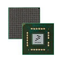
MPC8536DS Freescale Semiconductor, MPC8536DS Datasheet - Page 1357

MPC8536DS
Manufacturer Part Number
MPC8536DS
Description
BOARD DEV SYSTEM MPC8536E
Manufacturer
Freescale Semiconductor
Series
PowerQUICC III™r
Type
MPUr
Datasheets
1.MPC8536EBVTAVLA.pdf
(127 pages)
2.MPC8536EBVTAVLA.pdf
(1706 pages)
3.MPC8536DS.pdf
(2 pages)
4.MPC8536DS.pdf
(126 pages)
Specifications of MPC8536DS
Contents
Board, Software and Documentation
Processor Series
MPC85xx
Core
e500
Data Bus Width
32 bit
Maximum Clock Frequency
667 MHz
Operating Supply Voltage
- 0.3 V to + 1.21 V
Maximum Operating Temperature
+ 105 C
Data Ram Size
32 KB
Interface Type
SPI, USB
Program Memory Type
DDR2, DDR3, SDRAM
Core Size
32 Bit
Program Memory Size
544KB
Cpu Speed
1.5GHz
Digital Ic Case Style
BGA
No. Of Pins
783
Supply Voltage Range
0.95V To 1.05V
Rohs Compliant
Yes
For Use With/related Products
MPC8536
Lead Free Status / RoHS Status
Lead free / RoHS Compliant
- MPC8536EBVTAVLA PDF datasheet
- MPC8536EBVTAVLA PDF datasheet #2
- MPC8536DS PDF datasheet #3
- MPC8536DS PDF datasheet #4
- Current page: 1357 of 1706
- Download datasheet (15Mb)
21.3.2.12 ULPI Register Access (ULPI VIEWPORT)
The register provides indirect access to the ULPI PHY register set. Although the controller modules
perform access to the ULPI PHY register set, there may be extraordinary circumstances where software
may need direct access. Be advised that writes to the ULPI through the ULPI viewport can substantially
harm standard USB operations. Currently no usage model has been defined where software should need
to execute writes directly to the ULPI. Note that executing read operations though the ULPI viewport
should have no harmful side effects to standard USB operations. Also note that if the ULPI interface is not
enabled, this register will always read zeros.
ULPI VIEWPORT is shown in
Freescale Semiconductor
Offset 0x170
Reset
Reset
26–24
23–16
Bits
31
30
29
28
27
W
W
R
R
ULPIWU ULPIRUN ULPIRW
31
15
0
ULPIADDR
ULPIPORT
ULPIRUN
ULPIWU
ULPIRW
ULPISS
Name
—
30
0
MPC8536E PowerQUICC III Integrated Processor Reference Manual, Rev. 1
ULPIDATRD
Figure 21-18. ULPI Register Access (ULPI VIEWPORT)
29
0
ULPI Wake Up. Writing 1 to this bit begins the wakeup operation. This bit automatically
transitions to 0 after the wakeup is complete. Once this bit is set, it can not be cleared by
software.
Note: The driver must never execute a wakeup and a read/write operation at the same time.
ULPI Run. Writing 1 to this bit begins a read/write operation. This bit automatically transitions
to 0 after the read/write is complete. Once this bit is set, it can not be cleared by software.
Note: The driver must never execute a wakeup and a read/write operation at the same time.
This bit selects between running a read or write operation to the ULPI.
0 Read
1 Write
Reserved, should be cleared.
This bit represents the state of the ULPI interface. Before reading this bit, the ULPIPORT field
should be set accordingly if used with the multi-port host. Otherwise, this field should always
remain 0.
0 Any other state (that is, carkit, serial, low power).
1 Normal Sync State.
For wakeup or read/write operations this value selects the port number to which the ULPI PHY
is attached. Valid values are 0 and 1.
When a read or write operation is commanded, the address of the operation is written to this
field.
Table 21-20. ULPI VIEWPORT Field Descriptions
Figure
28
—
0
ULPISS
21-18.
27
n
26
ULPIPORT
0
0
All zeros
24
0
8
23
0
7
Description
0
0
ULPIDTWR
ULPIADDR
0
Universal Serial Bus Interfaces
0
0
Access: Mixed
0
21-23
16
0
0
Related parts for MPC8536DS
Image
Part Number
Description
Manufacturer
Datasheet
Request
R
Part Number:
Description:
Manufacturer:
Freescale Semiconductor, Inc
Datasheet:
Part Number:
Description:
Manufacturer:
Freescale Semiconductor, Inc
Datasheet:
Part Number:
Description:
Manufacturer:
Freescale Semiconductor, Inc
Datasheet:
Part Number:
Description:
Manufacturer:
Freescale Semiconductor, Inc
Datasheet:
Part Number:
Description:
Manufacturer:
Freescale Semiconductor, Inc
Datasheet:
Part Number:
Description:
Manufacturer:
Freescale Semiconductor, Inc
Datasheet:
Part Number:
Description:
Manufacturer:
Freescale Semiconductor, Inc
Datasheet:
Part Number:
Description:
Manufacturer:
Freescale Semiconductor, Inc
Datasheet:
Part Number:
Description:
Manufacturer:
Freescale Semiconductor, Inc
Datasheet:
Part Number:
Description:
Manufacturer:
Freescale Semiconductor, Inc
Datasheet:
Part Number:
Description:
Manufacturer:
Freescale Semiconductor, Inc
Datasheet:
Part Number:
Description:
Manufacturer:
Freescale Semiconductor, Inc
Datasheet:
Part Number:
Description:
Manufacturer:
Freescale Semiconductor, Inc
Datasheet:
Part Number:
Description:
Manufacturer:
Freescale Semiconductor, Inc
Datasheet:
Part Number:
Description:
Manufacturer:
Freescale Semiconductor, Inc
Datasheet:


