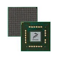
MPC8536DS Freescale Semiconductor, MPC8536DS Datasheet - Page 721

MPC8536DS
Manufacturer Part Number
MPC8536DS
Description
BOARD DEV SYSTEM MPC8536E
Manufacturer
Freescale Semiconductor
Series
PowerQUICC III™r
Type
MPUr
Datasheets
1.MPC8536EBVTAVLA.pdf
(127 pages)
2.MPC8536EBVTAVLA.pdf
(1706 pages)
3.MPC8536DS.pdf
(2 pages)
4.MPC8536DS.pdf
(126 pages)
Specifications of MPC8536DS
Contents
Board, Software and Documentation
Processor Series
MPC85xx
Core
e500
Data Bus Width
32 bit
Maximum Clock Frequency
667 MHz
Operating Supply Voltage
- 0.3 V to + 1.21 V
Maximum Operating Temperature
+ 105 C
Data Ram Size
32 KB
Interface Type
SPI, USB
Program Memory Type
DDR2, DDR3, SDRAM
Core Size
32 Bit
Program Memory Size
544KB
Cpu Speed
1.5GHz
Digital Ic Case Style
BGA
No. Of Pins
783
Supply Voltage Range
0.95V To 1.05V
Rohs Compliant
Yes
For Use With/related Products
MPC8536
Lead Free Status / RoHS Status
Lead free / RoHS Compliant
- MPC8536EBVTAVLA PDF datasheet
- MPC8536EBVTAVLA PDF datasheet #2
- MPC8536DS PDF datasheet #3
- MPC8536DS PDF datasheet #4
- Current page: 721 of 1706
- Download datasheet (15Mb)
13.4.4.2.1
The following example further illustrates the steps required to perform two writes to the RAM array at
non-sequential addresses assuming that the relevant BRn and ORn registers have been previously set up:
Note that if step 1 (or 6) and 2 (or 7) are reversed, step 3 (or 8) is replaced by the following:
13.4.4.2.2
RAM array contents may also be read for debug purposes, for example, by alternating dummy read
transactions, each time followed by reads of MDR (MxMR[OP] = 0b10). The following example further
illustrates the steps required to perform two reads from the RAM array at non-sequential addresses
assuming that the relevant BRn and ORn registers have been previously set up:
Freescale Semiconductor
1. Program MxMR for the first write (with the desired RAM array address).
2. Write pattern/data to MDR to ensure that the MxMR has already been updated with the desired
3. Read MDR to ensure that the MDR has already been updated with the desired pattern. (Or, read
4. Perform a dummy write transaction.
5. Read/check MxMR[MAD]. If incremented, the previous dummy write transaction is completed;
6. Program MxMR for the second write with the desired RAM array address.
7. Write pattern/data to MDR to ensure that the MxMR has already been updated with the desired
8. Read MDR to ensure that the MDR has already been updated with the desired pattern.
9. Perform a dummy write transaction.
10. Read/check MxMR[MAD]. If incremented, the previous dummy write transaction is completed.
•
1. Program MxMR for the first read with the desired RAM array address.
2. Read MxMR to ensure that the MxMR has already been updated with the desired configuration,
3. Perform a dummy read transaction.
4. Read/check MxMR[MAD]. If incremented, the previous dummy read transaction is completed;
5. Read MDR.
6. Program MxMR for the second read with the desired RAM array address.
7. Read MxMR to ensure that the MxMR has already been updated with the desired configuration,
8. Perform a dummy read transaction.
9. Read/check MxMR[MAD]. If incremented, the previous dummy read transaction is completed;
10. Read MDR.
configuration.
MxMR register if step 2 is not performed.)
proceed to step 6. Repeat step 5 until incremented.
configuration.
Read MxMR to ensure that the MxMR has already been updated with the desired configuration.
such as RAM array address.
proceed to step 5. Repeat step 4 until incremented.
such as RAM array address.
proceed to step 10. Repeat step 9 until incremented.
UPM Programming Example (Two Sequential Writes to the RAM Array)
UPM Programming Example (Two Sequential Reads from the RAM Array)
MPC8536E PowerQUICC III Integrated Processor Reference Manual, Rev. 1
Enhanced Local Bus Controller
13-79
Related parts for MPC8536DS
Image
Part Number
Description
Manufacturer
Datasheet
Request
R
Part Number:
Description:
Manufacturer:
Freescale Semiconductor, Inc
Datasheet:
Part Number:
Description:
Manufacturer:
Freescale Semiconductor, Inc
Datasheet:
Part Number:
Description:
Manufacturer:
Freescale Semiconductor, Inc
Datasheet:
Part Number:
Description:
Manufacturer:
Freescale Semiconductor, Inc
Datasheet:
Part Number:
Description:
Manufacturer:
Freescale Semiconductor, Inc
Datasheet:
Part Number:
Description:
Manufacturer:
Freescale Semiconductor, Inc
Datasheet:
Part Number:
Description:
Manufacturer:
Freescale Semiconductor, Inc
Datasheet:
Part Number:
Description:
Manufacturer:
Freescale Semiconductor, Inc
Datasheet:
Part Number:
Description:
Manufacturer:
Freescale Semiconductor, Inc
Datasheet:
Part Number:
Description:
Manufacturer:
Freescale Semiconductor, Inc
Datasheet:
Part Number:
Description:
Manufacturer:
Freescale Semiconductor, Inc
Datasheet:
Part Number:
Description:
Manufacturer:
Freescale Semiconductor, Inc
Datasheet:
Part Number:
Description:
Manufacturer:
Freescale Semiconductor, Inc
Datasheet:
Part Number:
Description:
Manufacturer:
Freescale Semiconductor, Inc
Datasheet:
Part Number:
Description:
Manufacturer:
Freescale Semiconductor, Inc
Datasheet:


