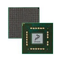
MPC8536DS Freescale Semiconductor, MPC8536DS Datasheet - Page 529

MPC8536DS
Manufacturer Part Number
MPC8536DS
Description
BOARD DEV SYSTEM MPC8536E
Manufacturer
Freescale Semiconductor
Series
PowerQUICC III™r
Type
MPUr
Datasheets
1.MPC8536EBVTAVLA.pdf
(127 pages)
2.MPC8536EBVTAVLA.pdf
(1706 pages)
3.MPC8536DS.pdf
(2 pages)
4.MPC8536DS.pdf
(126 pages)
Specifications of MPC8536DS
Contents
Board, Software and Documentation
Processor Series
MPC85xx
Core
e500
Data Bus Width
32 bit
Maximum Clock Frequency
667 MHz
Operating Supply Voltage
- 0.3 V to + 1.21 V
Maximum Operating Temperature
+ 105 C
Data Ram Size
32 KB
Interface Type
SPI, USB
Program Memory Type
DDR2, DDR3, SDRAM
Core Size
32 Bit
Program Memory Size
544KB
Cpu Speed
1.5GHz
Digital Ic Case Style
BGA
No. Of Pins
783
Supply Voltage Range
0.95V To 1.05V
Rohs Compliant
Yes
For Use With/related Products
MPC8536
Lead Free Status / RoHS Status
Lead free / RoHS Compliant
- MPC8536EBVTAVLA PDF datasheet
- MPC8536EBVTAVLA PDF datasheet #2
- MPC8536DS PDF datasheet #3
- MPC8536DS PDF datasheet #4
- Current page: 529 of 1706
- Download datasheet (15Mb)
Reset
Table 20-46
10.7.3.3
The key size register stores the number of valid bytes in the dynamic polynomial written to the key register
(Section 10.7.3.13, “CRCU Key
generated if a value other than zero, four or eight is written to the register. It is not necessary to write to
this register, as the polynomial size is clearly fixed by the algorithm. A context error is generated if this
register is written after processing has begun.
Freescale Semiconductor
Addr 0x3_F000
W
R
The following bits are described for information only. They are not under direct user control.
62-63
0–56
0
Bits
57
58
59
60
61
describes the CRCU mode register fields:
CRCU Key Size Register
Name
CICV
DOC
DOS
ALG
DIS
—
—
MPC8536E PowerQUICC III Integrated Processor Reference Manual, Rev. 1
Reserved
ICV Check. Selects whether a comparison between the computed CRC and the
residue should be performed.
0 Disabled.
1 Enable ICV check. Compares a CRC calculated across the message and received
Reserved
Disable Output Complement. Normal processing includes complementing the CRC
result.
0 Normal operation. CRC result is complemented..
1 Disable output complement.
Disable Output Swap. Normal processing includes a bit swap and byte swap of the
CRC result.
0 Normal operation. CRC result is bit swapped and byte swapped.
1 Disable output swapping.
Disable Input Swap. Normal processing includes a bit swap and byte swap of the input
data.
0 Normal operation. Input data is bit swapped and byte swapped.
1 Disable input swapping.
Algorithm. Selects the CRC algorithm mode for the CRCU.
00 IEEE 802 mode. The CRC32 algorithm will be performed using the polynomial
01 iSCSI mode. The CRC32c algorithm will be performed using the polynomial
10 Static custom mode. The CRC remainder will be computed using the Control
11 Dynamic custom mode. The CRC remainder will be computed using the Key
ICV against the stored residue. The comparison is performed prior to the bit
manipulations controlled by the DOS and DOC bits.
0x04C11DB7 and the residue 0xC704DD7B will be used for ICV checking.
0x1EDC6F41 and the residue 0x1C2D19ED will be used for ICV checking.
Register bits 32-63 as the polynomial and bits 0-31 as the residue.
Register bits 32-63 as the polynomial and bits 0-31 as the residue.
Register”). The reset value is zero, and an illegal key size error is
Figure 10-40. CRCU Mode Register
—
All zeros
Description
56
CICV — DOC DOS DIS ALG
57
58
Security Engine (SEC) 3.0
59
Access: Read/Write
60
61
10-99
62 63
Related parts for MPC8536DS
Image
Part Number
Description
Manufacturer
Datasheet
Request
R
Part Number:
Description:
Manufacturer:
Freescale Semiconductor, Inc
Datasheet:
Part Number:
Description:
Manufacturer:
Freescale Semiconductor, Inc
Datasheet:
Part Number:
Description:
Manufacturer:
Freescale Semiconductor, Inc
Datasheet:
Part Number:
Description:
Manufacturer:
Freescale Semiconductor, Inc
Datasheet:
Part Number:
Description:
Manufacturer:
Freescale Semiconductor, Inc
Datasheet:
Part Number:
Description:
Manufacturer:
Freescale Semiconductor, Inc
Datasheet:
Part Number:
Description:
Manufacturer:
Freescale Semiconductor, Inc
Datasheet:
Part Number:
Description:
Manufacturer:
Freescale Semiconductor, Inc
Datasheet:
Part Number:
Description:
Manufacturer:
Freescale Semiconductor, Inc
Datasheet:
Part Number:
Description:
Manufacturer:
Freescale Semiconductor, Inc
Datasheet:
Part Number:
Description:
Manufacturer:
Freescale Semiconductor, Inc
Datasheet:
Part Number:
Description:
Manufacturer:
Freescale Semiconductor, Inc
Datasheet:
Part Number:
Description:
Manufacturer:
Freescale Semiconductor, Inc
Datasheet:
Part Number:
Description:
Manufacturer:
Freescale Semiconductor, Inc
Datasheet:
Part Number:
Description:
Manufacturer:
Freescale Semiconductor, Inc
Datasheet:


