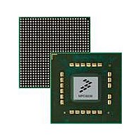
MPC8536DS Freescale Semiconductor, MPC8536DS Datasheet - Page 1086

MPC8536DS
Manufacturer Part Number
MPC8536DS
Description
BOARD DEV SYSTEM MPC8536E
Manufacturer
Freescale Semiconductor
Series
PowerQUICC III™r
Type
MPUr
Datasheets
1.MPC8536EBVTAVLA.pdf
(127 pages)
2.MPC8536EBVTAVLA.pdf
(1706 pages)
3.MPC8536DS.pdf
(2 pages)
4.MPC8536DS.pdf
(126 pages)
Specifications of MPC8536DS
Contents
Board, Software and Documentation
Processor Series
MPC85xx
Core
e500
Data Bus Width
32 bit
Maximum Clock Frequency
667 MHz
Operating Supply Voltage
- 0.3 V to + 1.21 V
Maximum Operating Temperature
+ 105 C
Data Ram Size
32 KB
Interface Type
SPI, USB
Program Memory Type
DDR2, DDR3, SDRAM
Core Size
32 Bit
Program Memory Size
544KB
Cpu Speed
1.5GHz
Digital Ic Case Style
BGA
No. Of Pins
783
Supply Voltage Range
0.95V To 1.05V
Rohs Compliant
Yes
For Use With/related Products
MPC8536
Lead Free Status / RoHS Status
Lead free / RoHS Compliant
- MPC8536EBVTAVLA PDF datasheet
- MPC8536EBVTAVLA PDF datasheet #2
- MPC8536DS PDF datasheet #3
- MPC8536DS PDF datasheet #4
- Current page: 1086 of 1706
- Download datasheet (15Mb)
PCI Bus Interface
To access the configuration space, a 32-bit value must be written to the PCI CFG_ADDR register that
specifies the target PCI bus, the target device on that bus, and the configuration register to be accessed
within that device. A read or write to the PCI CFG_DATA register causes the host bridge to translate the
access into a PCI configuration cycle (provided the enable bit in CONFIG_ADDR is set and the device
number is not 0b1_1111).
See
CFG_ADDR and
CFG_DATA.
16.4.2.11.2 Host Accessing the PCI Configuration Space
Power Architecture processor accesses to the PCI CFG_DATA register should use the load/store with
byte-reversed instructions.
Example: Configuration sequence, 4-byte data read from the revision ID/standard programming
interface/subclass code/class code registers at address offset 0x08 of the PCI configuration header (device
0 on the PCI bus 0 is the PCI controller itself).
Initial values:
Code sequence:
Results:
16-60
Offset (Hex)
0x34, 0x38
Address
0x2C
0x2E
0x3C
0x3D
0x3E
0x28
0x30
0x3F
Section 16.3.1.1.1, “PCI Configuration Address Register (CFG_ADDR),”
r0 contains 0x8000_0008
r1 contains CCSRBAR + BlockBase + 0x000 (Address of PCI CFG_ADDR register)
r2 contains CCSRBAR + BlockBase + 0x004 (Address of PCI CFG_DATA register)
r3 contains 0xFFFF_FFFF
Register at 0x08 contains 0x9988_7766 (0x0B to 0x08)
stw r0, 0 (r1)
ld r3, 0 (r2)
Address CCSRBAR + BlockBase + 0x000 contains 0x8000_0008
Register r3 contains 0x6677_8899
Subsystem Vendor ID
Expansion ROM base
Register Name
Subsystem ID
Section 16.3.1.1.2, “PCI Configuration Data Register (CFG_DATA),”
Interrupt line
Interrupt pin
Table 16-49. PCI Configuration Space Header Summary (continued)
Min_Gnt
Max_Lat
MPC8536E PowerQUICC III Integrated Processor Reference Manual, Rev. 1
address
—
—
Reserved for future use
Identifies the subsystem vendor ID
Identifies the subsystem ID
Base address and size information for expansion ROM contained in an add-on board
Reserved for future use
Contains interrupt line routing information
Indicates which interrupt pin the device (or function) uses
Specifies the length of the device’s burst period in 0.25 µs units
Specifies how often the device needs access to the bus in 0.25 µs units
Description
for details on PCI
Freescale Semiconductor
for details on PCI
Related parts for MPC8536DS
Image
Part Number
Description
Manufacturer
Datasheet
Request
R
Part Number:
Description:
Manufacturer:
Freescale Semiconductor, Inc
Datasheet:
Part Number:
Description:
Manufacturer:
Freescale Semiconductor, Inc
Datasheet:
Part Number:
Description:
Manufacturer:
Freescale Semiconductor, Inc
Datasheet:
Part Number:
Description:
Manufacturer:
Freescale Semiconductor, Inc
Datasheet:
Part Number:
Description:
Manufacturer:
Freescale Semiconductor, Inc
Datasheet:
Part Number:
Description:
Manufacturer:
Freescale Semiconductor, Inc
Datasheet:
Part Number:
Description:
Manufacturer:
Freescale Semiconductor, Inc
Datasheet:
Part Number:
Description:
Manufacturer:
Freescale Semiconductor, Inc
Datasheet:
Part Number:
Description:
Manufacturer:
Freescale Semiconductor, Inc
Datasheet:
Part Number:
Description:
Manufacturer:
Freescale Semiconductor, Inc
Datasheet:
Part Number:
Description:
Manufacturer:
Freescale Semiconductor, Inc
Datasheet:
Part Number:
Description:
Manufacturer:
Freescale Semiconductor, Inc
Datasheet:
Part Number:
Description:
Manufacturer:
Freescale Semiconductor, Inc
Datasheet:
Part Number:
Description:
Manufacturer:
Freescale Semiconductor, Inc
Datasheet:
Part Number:
Description:
Manufacturer:
Freescale Semiconductor, Inc
Datasheet:


