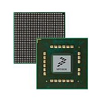
MPC8536DS Freescale Semiconductor, MPC8536DS Datasheet - Page 222

MPC8536DS
Manufacturer Part Number
MPC8536DS
Description
BOARD DEV SYSTEM MPC8536E
Manufacturer
Freescale Semiconductor
Series
PowerQUICC III™r
Type
MPUr
Datasheets
1.MPC8536EBVTAVLA.pdf
(127 pages)
2.MPC8536EBVTAVLA.pdf
(1706 pages)
3.MPC8536DS.pdf
(2 pages)
4.MPC8536DS.pdf
(126 pages)
Specifications of MPC8536DS
Contents
Board, Software and Documentation
Processor Series
MPC85xx
Core
e500
Data Bus Width
32 bit
Maximum Clock Frequency
667 MHz
Operating Supply Voltage
- 0.3 V to + 1.21 V
Maximum Operating Temperature
+ 105 C
Data Ram Size
32 KB
Interface Type
SPI, USB
Program Memory Type
DDR2, DDR3, SDRAM
Core Size
32 Bit
Program Memory Size
544KB
Cpu Speed
1.5GHz
Digital Ic Case Style
BGA
No. Of Pins
783
Supply Voltage Range
0.95V To 1.05V
Rohs Compliant
Yes
For Use With/related Products
MPC8536
Lead Free Status / RoHS Status
Lead free / RoHS Compliant
- MPC8536EBVTAVLA PDF datasheet
- MPC8536EBVTAVLA PDF datasheet #2
- MPC8536DS PDF datasheet #3
- MPC8536DS PDF datasheet #4
- Current page: 222 of 1706
- Download datasheet (15Mb)
L2 Look-Aside Cache/SRAM
6.1.1
The L2 cache has the following characteristics:
6-2
•
•
•
•
•
•
•
•
•
•
•
•
•
Supports 36-bit address space
Write-through, front-side cache
— Front-side design provides easier cache access for the I/O masters, such as Ethernet
— Write-through design is more efficient on the processor bus for front-side caches
Valid, locked, and stale states (no modified state)
Two input data buses (64 and 128 bits wide) and one output data bus (128 bits wide)
All accesses are fully pipelined and non-blocking (allows hits under misses)
512-Kbyte array organized as 2048 eight-way sets of 32-byte cache lines
Eight-way set associativity with a pseudo-LRU (7-bit) replacement algorithm.
— High level of associativity yields good performance even with many lines locked or used as
I/O devices can store data into the cache in a process called ‘stashing.’
— Stashing is indicated for global I/O writes either by a transaction attribute or by a
— Regions of the cache can be reserved exclusively for stashing to prevent pollution of processor
Processor L2 cache regions are configurable to allocate instructions, data, or both.
— External masters can force data to be allocated into the cache through programmed memory
Data ECC on 64-bit boundaries (single-error correction, double-error detection)
Tag arrays use 20 tag bits and 1 tag parity bit per line.
Multiple cache locking methods supported
— Individual line locks are set and cleared using e500 cache locking APU instructions—Data
— A lock attribute can be attached to write operations.
— Individual line locks are set and cleared through core-initiated instructions, by external reads
— The entire cache can be locked by setting a configuration register appropriately.
Lock clearing methods
— Individual locks can be cleared by cache-locking APU instructions—Data Cache Block Lock
— Flash clearing of all instruction and/or data locks is done by writes to configuration registers.
— An unlock attribute can be attached to a read instruction.
SRAM regions
programmable memory range
cache regions.
ranges or special transaction types (stashing).
– 1, 2, or 4 ways can be configured for stashing only
Cache Block Touch and Lock Set (dcbtls), Data Cache Block Touch for Store and Lock Set
(dcbtstls), and Instruction Cache Block Touch and Lock Set (icbtls).
or writes, or by accesses to programmed memory ranges defined in L2 cache external write
address registers (L2CEWARn).
Clear (dcblc) and Instruction Cache Block Lock Clear (icblc)—or by a snooped flush unless
entire cache is locked.
L2 Cache and SRAM Features
MPC8536E PowerQUICC III Integrated Processor Reference Manual, Rev. 1
Freescale Semiconductor
Related parts for MPC8536DS
Image
Part Number
Description
Manufacturer
Datasheet
Request
R
Part Number:
Description:
Manufacturer:
Freescale Semiconductor, Inc
Datasheet:
Part Number:
Description:
Manufacturer:
Freescale Semiconductor, Inc
Datasheet:
Part Number:
Description:
Manufacturer:
Freescale Semiconductor, Inc
Datasheet:
Part Number:
Description:
Manufacturer:
Freescale Semiconductor, Inc
Datasheet:
Part Number:
Description:
Manufacturer:
Freescale Semiconductor, Inc
Datasheet:
Part Number:
Description:
Manufacturer:
Freescale Semiconductor, Inc
Datasheet:
Part Number:
Description:
Manufacturer:
Freescale Semiconductor, Inc
Datasheet:
Part Number:
Description:
Manufacturer:
Freescale Semiconductor, Inc
Datasheet:
Part Number:
Description:
Manufacturer:
Freescale Semiconductor, Inc
Datasheet:
Part Number:
Description:
Manufacturer:
Freescale Semiconductor, Inc
Datasheet:
Part Number:
Description:
Manufacturer:
Freescale Semiconductor, Inc
Datasheet:
Part Number:
Description:
Manufacturer:
Freescale Semiconductor, Inc
Datasheet:
Part Number:
Description:
Manufacturer:
Freescale Semiconductor, Inc
Datasheet:
Part Number:
Description:
Manufacturer:
Freescale Semiconductor, Inc
Datasheet:
Part Number:
Description:
Manufacturer:
Freescale Semiconductor, Inc
Datasheet:


