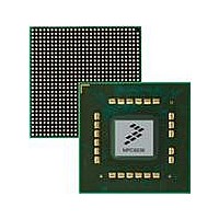
MPC8536DS Freescale Semiconductor, MPC8536DS Datasheet - Page 218

MPC8536DS
Manufacturer Part Number
MPC8536DS
Description
BOARD DEV SYSTEM MPC8536E
Manufacturer
Freescale Semiconductor
Series
PowerQUICC III™r
Type
MPUr
Datasheets
1.MPC8536EBVTAVLA.pdf
(127 pages)
2.MPC8536EBVTAVLA.pdf
(1706 pages)
3.MPC8536DS.pdf
(2 pages)
4.MPC8536DS.pdf
(126 pages)
Specifications of MPC8536DS
Contents
Board, Software and Documentation
Processor Series
MPC85xx
Core
e500
Data Bus Width
32 bit
Maximum Clock Frequency
667 MHz
Operating Supply Voltage
- 0.3 V to + 1.21 V
Maximum Operating Temperature
+ 105 C
Data Ram Size
32 KB
Interface Type
SPI, USB
Program Memory Type
DDR2, DDR3, SDRAM
Core Size
32 Bit
Program Memory Size
544KB
Cpu Speed
1.5GHz
Digital Ic Case Style
BGA
No. Of Pins
783
Supply Voltage Range
0.95V To 1.05V
Rohs Compliant
Yes
For Use With/related Products
MPC8536
Lead Free Status / RoHS Status
Lead free / RoHS Compliant
- MPC8536EBVTAVLA PDF datasheet
- MPC8536EBVTAVLA PDF datasheet #2
- MPC8536DS PDF datasheet #3
- MPC8536DS PDF datasheet #4
- Current page: 218 of 1706
- Download datasheet (15Mb)
e500 Core Integration Details
The “Core Complex Bus (CCB) and System Integration” chapter of the core document describes the
signals that are shown in
5.3
Table 5-1
organized into two sections:
5-4
Cache protocol
Clocking
•
•
•
•
•
•
Feature
e500 coherency module (ECM). The ECM, described in
facilitates communication between the core, the L2 cache, and the other blocks that comprise the
coherent memory domain of the SoC.
The ECM provides a mechanism for I/O-initiated transactions to snoop the core complex bus
(CCB) of the core to maintain coherency across cacheable local memory. It also provides a flexible,
easily expandable switch-type structure for core- and I/O-initiated transactions to be routed
(dispatched) to target modules on the device. The CCB is described in the “Core Complex Bus
(CCB) and System Integration” chapter of the e500 Reference Manual.
Interrupts. The e500 core handles the hardware interrupts that are generated from SoC peripheral
logic, typically by error conditions encountered from within blocks on the integrated device.
Chapter 9, “Programmable Interrupt Controller (PIC),”
controller, which prioritizes interrupt requests to the core.
interface with the PIC.
Power management. The core’s HID0[NAP, DOZE,SLEEP] can be used to assert nap, doze, and
sleep output signals to initiate power-saving modes at the integrated device level.
the e500 signals, which interact with the S0C level power management logic described in
Chapter 23, “Global Utilities.”
System debug. The architecture defines many features for software and hardware debug that
interact with the SoC.
features and watchpoint monitor.
block. The e500 Reference Manual describes how the architecture-defined debug resources are
implemented on the e500 core.
“General Feature Integration Details”
“Register Model Integration Details”
the SoC’s implementation of the core register model.
Table 5-1. Differences Between the e500 Core and the PowerQUICC III Core Implementation
summarizes details of the PowerQUICC III–specific implementation of the e500 core. It is
Summary of Core Integratation Details
The write-through L2 cache implemented on the SoC does not support MESI cache protocol.
Internal clock multipliers ranging from 1 to 8 times the bus clock, including integer and half-mode
multipliers.The integrated device supports multipliers of 2, 2.5, 3, and 3.5 See the table entry,
Implementation.
MPC8536E PowerQUICC III Integrated Processor Reference Manual, Rev. 1
Figure 5-2
Chapter 25, “Debug Features and Watchpoint Facility,”
and other aspects of core integration.
General Feature Integration Details
Figure 5-2
summarizes how integration-specific details are reflected in
summarizes integration-specific details by functionality.
PowerQUICC III Implementation
shows the e500 signals that interface with the debug
describes the programmable interrupt
Chapter 7, “e500 Coherency Module,”
Figure 5-2
shows the e500 signals that
Freescale Semiconductor
describes the debug
Figure 5-2
HID1
shows
Related parts for MPC8536DS
Image
Part Number
Description
Manufacturer
Datasheet
Request
R
Part Number:
Description:
Manufacturer:
Freescale Semiconductor, Inc
Datasheet:
Part Number:
Description:
Manufacturer:
Freescale Semiconductor, Inc
Datasheet:
Part Number:
Description:
Manufacturer:
Freescale Semiconductor, Inc
Datasheet:
Part Number:
Description:
Manufacturer:
Freescale Semiconductor, Inc
Datasheet:
Part Number:
Description:
Manufacturer:
Freescale Semiconductor, Inc
Datasheet:
Part Number:
Description:
Manufacturer:
Freescale Semiconductor, Inc
Datasheet:
Part Number:
Description:
Manufacturer:
Freescale Semiconductor, Inc
Datasheet:
Part Number:
Description:
Manufacturer:
Freescale Semiconductor, Inc
Datasheet:
Part Number:
Description:
Manufacturer:
Freescale Semiconductor, Inc
Datasheet:
Part Number:
Description:
Manufacturer:
Freescale Semiconductor, Inc
Datasheet:
Part Number:
Description:
Manufacturer:
Freescale Semiconductor, Inc
Datasheet:
Part Number:
Description:
Manufacturer:
Freescale Semiconductor, Inc
Datasheet:
Part Number:
Description:
Manufacturer:
Freescale Semiconductor, Inc
Datasheet:
Part Number:
Description:
Manufacturer:
Freescale Semiconductor, Inc
Datasheet:
Part Number:
Description:
Manufacturer:
Freescale Semiconductor, Inc
Datasheet:


