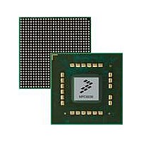
MPC8536DS Freescale Semiconductor, MPC8536DS Datasheet - Page 1073

MPC8536DS
Manufacturer Part Number
MPC8536DS
Description
BOARD DEV SYSTEM MPC8536E
Manufacturer
Freescale Semiconductor
Series
PowerQUICC III™r
Type
MPUr
Datasheets
1.MPC8536EBVTAVLA.pdf
(127 pages)
2.MPC8536EBVTAVLA.pdf
(1706 pages)
3.MPC8536DS.pdf
(2 pages)
4.MPC8536DS.pdf
(126 pages)
Specifications of MPC8536DS
Contents
Board, Software and Documentation
Processor Series
MPC85xx
Core
e500
Data Bus Width
32 bit
Maximum Clock Frequency
667 MHz
Operating Supply Voltage
- 0.3 V to + 1.21 V
Maximum Operating Temperature
+ 105 C
Data Ram Size
32 KB
Interface Type
SPI, USB
Program Memory Type
DDR2, DDR3, SDRAM
Core Size
32 Bit
Program Memory Size
544KB
Cpu Speed
1.5GHz
Digital Ic Case Style
BGA
No. Of Pins
783
Supply Voltage Range
0.95V To 1.05V
Rohs Compliant
Yes
For Use With/related Products
MPC8536
Lead Free Status / RoHS Status
Lead free / RoHS Compliant
- MPC8536EBVTAVLA PDF datasheet
- MPC8536EBVTAVLA PDF datasheet #2
- MPC8536DS PDF datasheet #3
- MPC8536DS PDF datasheet #4
- Current page: 1073 of 1706
- Download datasheet (15Mb)
16.4.2.3
PCI defines three physical address spaces—PCI memory space, PCI I/O space, and PCI configuration
space. Access to the PCI memory and I/O space is straightforward, although one must take into account
the local memory access window and address translation being used. The address translation registers are
described in
described in
Address decoding on the PCI bus is performed by every device for every PCI transaction. Each agent is
responsible for decoding its own address. PCI supports two types of address decoding—positive decoding
and subtractive decoding. For positive decoding, each device looks for accesses in the address range that
the device has been assigned. For subtractive decoding, one device on the bus looks for accesses that no
other device has claimed. See
transactions.
The information contained in the two low-order address bits (PCI_AD[1:0]) varies by the address space
(memory, I/O, or configuration). Regardless of the encoding scheme, the two low-order address bits are
always included in parity calculations.
16.4.2.3.1
For memory accesses, PCI defines two types of burst ordering controlled by the two low-order bits of the
address—linear incrementing (PCI_AD[1:0] = 0b00) and cache wrap mode (PCI_AD[1:0] = 0b10), as
shown in
initiator, the PCI controller always encodes PCI_AD[1:0] = 00 for PCI memory space accesses. As a
target, the PCI controller executes a target disconnect after the first data phase completes if
PCI_AD[1:0] = 01 or PCI_AD[1:0] = 0b11 during the address phase of a local memory access. See
Section 16.4.2.8.2, “Target-Initiated Termination,”
Freescale Semiconductor
1
BE[3:0]
PCI_C/
1110
1111
Reserved command encodings are reserved for future use. The PCI controller does not respond to these commands.
Memory-read-
line
Memory-write-
and-invalidate
Table
Command
PCI Bus
Section 16.3.1, “PCI Memory-Mapped Registers.”
Section 16.4.2.11, “Configuration Cycles.”
Addressing
Memory Space Addressing
16-48. The other two PCI_AD[1:0] possibilities (0b01 and 0b11) are reserved. As an
MPC8536E PowerQUICC III Integrated Processor Reference Manual, Rev. 1
00
01
Supported
PCI_AD[1:0]
Initiator
as an
Linear
Reserved
Yes
Table 16-48. Supported Combinations of PCI_AD[1:0]
No
Section 16.4.2.4, “Device Selection,”
Table 16-47. PCI Bus Commands (continued)
as a Target
Supported
Yes
Yes
Read
TD
Indicates that an initiator is requesting the transfer of an entire cache
line. This occurs only when the processor is performing a burst read.
Note that these processors perform burst reads only when the
appropriate cache is enabled and the transaction is not cache-inhibited.
Indicates that an initiator is transferring an entire cache line; if this data
is in any cacheable memory, that cache line needs to be invalidated.
Target
for more information on target disconnect conditions.
Write
TD
Access to the PCI configuration space is
Read
for information about claiming
—
Definition
Initiator
Write
—
PCI Bus Interface
16-47
Related parts for MPC8536DS
Image
Part Number
Description
Manufacturer
Datasheet
Request
R
Part Number:
Description:
Manufacturer:
Freescale Semiconductor, Inc
Datasheet:
Part Number:
Description:
Manufacturer:
Freescale Semiconductor, Inc
Datasheet:
Part Number:
Description:
Manufacturer:
Freescale Semiconductor, Inc
Datasheet:
Part Number:
Description:
Manufacturer:
Freescale Semiconductor, Inc
Datasheet:
Part Number:
Description:
Manufacturer:
Freescale Semiconductor, Inc
Datasheet:
Part Number:
Description:
Manufacturer:
Freescale Semiconductor, Inc
Datasheet:
Part Number:
Description:
Manufacturer:
Freescale Semiconductor, Inc
Datasheet:
Part Number:
Description:
Manufacturer:
Freescale Semiconductor, Inc
Datasheet:
Part Number:
Description:
Manufacturer:
Freescale Semiconductor, Inc
Datasheet:
Part Number:
Description:
Manufacturer:
Freescale Semiconductor, Inc
Datasheet:
Part Number:
Description:
Manufacturer:
Freescale Semiconductor, Inc
Datasheet:
Part Number:
Description:
Manufacturer:
Freescale Semiconductor, Inc
Datasheet:
Part Number:
Description:
Manufacturer:
Freescale Semiconductor, Inc
Datasheet:
Part Number:
Description:
Manufacturer:
Freescale Semiconductor, Inc
Datasheet:
Part Number:
Description:
Manufacturer:
Freescale Semiconductor, Inc
Datasheet:


