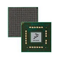
MPC8536DS Freescale Semiconductor, MPC8536DS Datasheet - Page 368

MPC8536DS
Manufacturer Part Number
MPC8536DS
Description
BOARD DEV SYSTEM MPC8536E
Manufacturer
Freescale Semiconductor
Series
PowerQUICC III™r
Type
MPUr
Datasheets
1.MPC8536EBVTAVLA.pdf
(127 pages)
2.MPC8536EBVTAVLA.pdf
(1706 pages)
3.MPC8536DS.pdf
(2 pages)
4.MPC8536DS.pdf
(126 pages)
Specifications of MPC8536DS
Contents
Board, Software and Documentation
Processor Series
MPC85xx
Core
e500
Data Bus Width
32 bit
Maximum Clock Frequency
667 MHz
Operating Supply Voltage
- 0.3 V to + 1.21 V
Maximum Operating Temperature
+ 105 C
Data Ram Size
32 KB
Interface Type
SPI, USB
Program Memory Type
DDR2, DDR3, SDRAM
Core Size
32 Bit
Program Memory Size
544KB
Cpu Speed
1.5GHz
Digital Ic Case Style
BGA
No. Of Pins
783
Supply Voltage Range
0.95V To 1.05V
Rohs Compliant
Yes
For Use With/related Products
MPC8536
Lead Free Status / RoHS Status
Lead free / RoHS Compliant
- MPC8536EBVTAVLA PDF datasheet
- MPC8536EBVTAVLA PDF datasheet #2
- MPC8536DS PDF datasheet #3
- MPC8536DS PDF datasheet #4
- Current page: 368 of 1706
- Download datasheet (15Mb)
DDR Memory Controller
8.6.2
After configuration of all parameters is complete, system software must set
DDR_SDRAM_CFG[MEM_EN] to enable the memory interface. Note that 200 s (500 s for DDR3)
must elapse after DRAM clocks are stable (DDR_SDRAM_CLK_CNTL[CLK_ADJUST] is set and any
chip select is enabled) before MEM_EN can be set, so a delay loop in the initialization code may be
necessary if software is enabling the memory controller. If DDR_SDRAM_CFG[BI] is not set, the DDR
memory controller conducts an automatic initialization sequence to the memory, which follows the
memory specifications. If the bypass initialization mode is used, then software can initialize the memory
through the DDR_SDRAM_MD_CNTL register.
8.6.3
This section describes the options offered by this device to support battery-backed main memory.
8.6.3.1
An external voltage sense device can be connected to this device through one of the external interrupt lines
IRQn. The external interrupt from the voltage sensor would then be steered through this device’s
programmable interrupt controller (PIC) to the IRQ_OUT signal. Note that the IRQ_OUT signal must
remain high until power is removed.
If DDR_SDRAM_CFG_2[SR_IE] is set, the IRQ_OUT signal from the interrupt controller is then
automatically detected by the DDR controller, which immediately causes main memory to enter
self-refresh mode. See
(DDR_SDRAM_CFG_2),”
8-94
WRLVL_EN
Parameter
BSTOPR
DDR SDRAM Initialization Sequence
Using Forced Self-Refresh Mode to Implement a Battery-Backed
RAM System
Hardware Based Self-Refresh
Table 8-69. Programming Differences Between Memory Types (continued)
Write Leveling Enable
Burst To Precharge Interval DDR2
MPC8536E PowerQUICC III Integrated Processor Reference Manual, Rev. 1
Section 8.4.1.9, “DDR SDRAM Control Configuration 2
Description
for further information on this bit.
DDR2
DDR3
DDR3
Should be set to 0
Can be set to 1 if write leveling is desired.
Otherwise the value used in
TIMING_CFG_2[WR_DATA_DELAY] is used to
shift all bytes during writes to DRAM. If write
leveling is used, all other fields in
DDR_WRLVL_CNTL should be programmed
appropriately based on the DRAM specifications.
application. Auto precharge can be enabled by
setting this field to all 0s.
application. Auto precharge can be enabled by
setting this field to all 0s.
Can be set to any value, depending on the
Can be set to any value, depending on the
Differences
Freescale Semiconductor
Section/page
8.4.1.21/8-40
8.4.1.13/8-33
Related parts for MPC8536DS
Image
Part Number
Description
Manufacturer
Datasheet
Request
R
Part Number:
Description:
Manufacturer:
Freescale Semiconductor, Inc
Datasheet:
Part Number:
Description:
Manufacturer:
Freescale Semiconductor, Inc
Datasheet:
Part Number:
Description:
Manufacturer:
Freescale Semiconductor, Inc
Datasheet:
Part Number:
Description:
Manufacturer:
Freescale Semiconductor, Inc
Datasheet:
Part Number:
Description:
Manufacturer:
Freescale Semiconductor, Inc
Datasheet:
Part Number:
Description:
Manufacturer:
Freescale Semiconductor, Inc
Datasheet:
Part Number:
Description:
Manufacturer:
Freescale Semiconductor, Inc
Datasheet:
Part Number:
Description:
Manufacturer:
Freescale Semiconductor, Inc
Datasheet:
Part Number:
Description:
Manufacturer:
Freescale Semiconductor, Inc
Datasheet:
Part Number:
Description:
Manufacturer:
Freescale Semiconductor, Inc
Datasheet:
Part Number:
Description:
Manufacturer:
Freescale Semiconductor, Inc
Datasheet:
Part Number:
Description:
Manufacturer:
Freescale Semiconductor, Inc
Datasheet:
Part Number:
Description:
Manufacturer:
Freescale Semiconductor, Inc
Datasheet:
Part Number:
Description:
Manufacturer:
Freescale Semiconductor, Inc
Datasheet:
Part Number:
Description:
Manufacturer:
Freescale Semiconductor, Inc
Datasheet:


