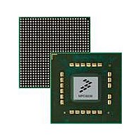
MPC8536DS Freescale Semiconductor, MPC8536DS Datasheet - Page 657

MPC8536DS
Manufacturer Part Number
MPC8536DS
Description
BOARD DEV SYSTEM MPC8536E
Manufacturer
Freescale Semiconductor
Series
PowerQUICC III™r
Type
MPUr
Datasheets
1.MPC8536EBVTAVLA.pdf
(127 pages)
2.MPC8536EBVTAVLA.pdf
(1706 pages)
3.MPC8536DS.pdf
(2 pages)
4.MPC8536DS.pdf
(126 pages)
Specifications of MPC8536DS
Contents
Board, Software and Documentation
Processor Series
MPC85xx
Core
e500
Data Bus Width
32 bit
Maximum Clock Frequency
667 MHz
Operating Supply Voltage
- 0.3 V to + 1.21 V
Maximum Operating Temperature
+ 105 C
Data Ram Size
32 KB
Interface Type
SPI, USB
Program Memory Type
DDR2, DDR3, SDRAM
Core Size
32 Bit
Program Memory Size
544KB
Cpu Speed
1.5GHz
Digital Ic Case Style
BGA
No. Of Pins
783
Supply Voltage Range
0.95V To 1.05V
Rohs Compliant
Yes
For Use With/related Products
MPC8536
Lead Free Status / RoHS Status
Lead free / RoHS Compliant
- MPC8536EBVTAVLA PDF datasheet
- MPC8536EBVTAVLA PDF datasheet #2
- MPC8536DS PDF datasheet #3
- MPC8536DS PDF datasheet #4
- Current page: 657 of 1706
- Download datasheet (15Mb)
Freescale Semiconductor
21–22
24–27
Bits
23
28
29
Name
XACS Extra address to chip-select setup. Setting this bit increases the delay of the LCS n assertion relative to the
TRLX
SETA
ACS
SCY
Address to chip-select setup. Determines the delay of the LCS n assertion relative to the address change
when the external memory access is handled by the GPCM. At system reset, OR0[ACS] = 11.
address change when the external memory access is handled by the GPCM. After a system reset,
OR0[XACS] = 1.
0 Address to chip-select setup is determined by ORx[ACS].
1 Address to chip-select setup is extended (see
Cycle length in bus clocks. Determines the number of wait states inserted in the bus cycle, when the GPCM
handles the external memory access. Thus it is the main parameter for determining cycle length. The total
cycle length depends on other timing attribute settings. After a system reset, OR0[SCY] = 1111.
0000 No wait states
0001 1 bus clock cycle wait state
...
1111 15 bus clock cycle wait states
External address termination.
0 Access is terminated internally by the memory controller unless the external device asserts LGTA earlier
1 Access is terminated externally by asserting the LGTA external pin. (Only LGTA can terminate the access).
Timing relaxed. Modifies the settings of timing parameters for slow memories or peripherals.
0 Normal timing is generated by the GPCM.
1 Relaxed timing on the following parameters:
• Adds an additional cycle between the address and control signals (only if ACS is not equal to 00).
• Doubles the number of wait states specified by SCY, providing up to 30 wait states.
• Works in conjunction with EHTR to extend hold time on read accesses.
• LCS n (only if ACS is not equal to 00) and LWE signals are negated one cycle earlier during writes.
to terminate the access.
MPC8536E PowerQUICC III Integrated Processor Reference Manual, Rev. 1
Value
Table 13-7. OR n
00
01
10
11
LCS n is output at the same time as the address lines. Note that this overrides the
value of CSNT such that CSNT = 0.
Reserved.
LCS n is output one quarter bus clock cycle after the address lines.
LCS n is output one half bus clock cycle after the address lines.
—
GPCM Field Descriptions (continued)
Description
Table 13-32
Meaning
and
Table
13-33).
Enhanced Local Bus Controller
13-15
Related parts for MPC8536DS
Image
Part Number
Description
Manufacturer
Datasheet
Request
R
Part Number:
Description:
Manufacturer:
Freescale Semiconductor, Inc
Datasheet:
Part Number:
Description:
Manufacturer:
Freescale Semiconductor, Inc
Datasheet:
Part Number:
Description:
Manufacturer:
Freescale Semiconductor, Inc
Datasheet:
Part Number:
Description:
Manufacturer:
Freescale Semiconductor, Inc
Datasheet:
Part Number:
Description:
Manufacturer:
Freescale Semiconductor, Inc
Datasheet:
Part Number:
Description:
Manufacturer:
Freescale Semiconductor, Inc
Datasheet:
Part Number:
Description:
Manufacturer:
Freescale Semiconductor, Inc
Datasheet:
Part Number:
Description:
Manufacturer:
Freescale Semiconductor, Inc
Datasheet:
Part Number:
Description:
Manufacturer:
Freescale Semiconductor, Inc
Datasheet:
Part Number:
Description:
Manufacturer:
Freescale Semiconductor, Inc
Datasheet:
Part Number:
Description:
Manufacturer:
Freescale Semiconductor, Inc
Datasheet:
Part Number:
Description:
Manufacturer:
Freescale Semiconductor, Inc
Datasheet:
Part Number:
Description:
Manufacturer:
Freescale Semiconductor, Inc
Datasheet:
Part Number:
Description:
Manufacturer:
Freescale Semiconductor, Inc
Datasheet:
Part Number:
Description:
Manufacturer:
Freescale Semiconductor, Inc
Datasheet:


