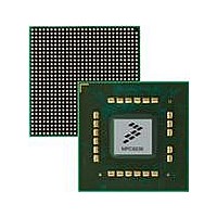
MPC8536DS Freescale Semiconductor, MPC8536DS Datasheet - Page 538

MPC8536DS
Manufacturer Part Number
MPC8536DS
Description
BOARD DEV SYSTEM MPC8536E
Manufacturer
Freescale Semiconductor
Series
PowerQUICC III™r
Type
MPUr
Datasheets
1.MPC8536EBVTAVLA.pdf
(127 pages)
2.MPC8536EBVTAVLA.pdf
(1706 pages)
3.MPC8536DS.pdf
(2 pages)
4.MPC8536DS.pdf
(126 pages)
Specifications of MPC8536DS
Contents
Board, Software and Documentation
Processor Series
MPC85xx
Core
e500
Data Bus Width
32 bit
Maximum Clock Frequency
667 MHz
Operating Supply Voltage
- 0.3 V to + 1.21 V
Maximum Operating Temperature
+ 105 C
Data Ram Size
32 KB
Interface Type
SPI, USB
Program Memory Type
DDR2, DDR3, SDRAM
Core Size
32 Bit
Program Memory Size
544KB
Cpu Speed
1.5GHz
Digital Ic Case Style
BGA
No. Of Pins
783
Supply Voltage Range
0.95V To 1.05V
Rohs Compliant
Yes
For Use With/related Products
MPC8536
Lead Free Status / RoHS Status
Lead free / RoHS Compliant
- MPC8536EBVTAVLA PDF datasheet
- MPC8536EBVTAVLA PDF datasheet #2
- MPC8536DS PDF datasheet #3
- MPC8536DS PDF datasheet #4
- Current page: 538 of 1706
- Download datasheet (15Mb)
Offset 0x3_F100
Reset 1
Security Engine (SEC) 3.0
If the CRCU is in both disable output complement mode (DOC bit is 1) and disable output swap mode
(DOS bit is 1), this register holds the uncomplemented and unswapped CRC remainder, as shown in
Figure
performing ICV checking. This form can also be written back to the CRCU after reset to continue a partial
CRC operation.
10.7.3.13 CRCU Key Register
The CRCU key register stores the polynomial and residue for the dynamic custom mode as set in the mode
register (see
coefficients. The reset value of this register is all zeros with a one in bit position 0. This register is dynamic,
in that it is reset by performing a re-initialize or a software reset. This allows a custom polynomial to be
used for specific processing without changing the platform-specific static custom polynomial stored in the
control register (see
programmed unless ICV checking is being performed. A context error is generated if this register is written
after processing has begun. A polynomial error is generated if a value is written to this register which does
not have a one in bit position 0.
10.7.3.14 CRCU FIFO
Words written to this address range are pushed onto the CRCU input FIFO, thereby buffering them for
processing. Partial words and misaligned data can be written to this address and it is automatically
realigned based on a big endian byte order.
10.7.4
This section contains details about the Data Encryption Standard execution unit (DEU), including modes
of operation, status and control registers, and FIFOs.
10-108
Offset 0x3_F400
W
R
x
W
W
R
R
0
31
g
r
32
32
x
10-54. This form is the one used internally to match against the polynomial specific residue when
31
31
1
1
30
g
r
x
33
33
30
30
2
1
29
Data Encryption Standard Execution Unit (DEU)
Figure 10-54. CRCU Context Register, Upper Half (Read in DOC and DOS Modes)
Section 10.7.3.2, “CRCU Mode
g
x
r
34
34
29
1
3
28
29
x
g
r
35
35
4
1
27
28
28
MPC8536E PowerQUICC III Integrated Processor Reference Manual, Rev. 1
Section 10.7.3.6, “CRCU Control
x
g
r
1
5
26
36
36
27
27
x
g
1
6
25
r
37
37
26
26
x
1
7
24
g
r
38
38
25
25
x
8
23
g
r
39
39
24
24
x
1
Figure 10-55. CRCU Key Register
9
22
40
40
x
10
1
21
x
11
1
20
Register”).
x
12
1
19
x
13
1
18
x
14
1
17
Register”). A residue does not need to be
x
Figure 10-55
15
1
—
—
16
x
16
15
x
17
1
14
x
18
1
13
shows the bit position of each
x
19
1
12
x
20
1
11
x
55 56 57 58 59 60 61 62 63
55 56 57 58 59 60 61 62 63
21 22 23 24 25 26 27 28 29 30 31
1
10
g
r
x
1 1 1 1 1 1 1 1 1 1
7
7
9
Freescale Semiconductor
x
g
r
8
6
6
x
g
r
7
5
Access: Read/Write
5
x
g
6
r
Access: Read/Write
4
4
x
5
g
r
3
3
x
4
g
r
2
x
2
3
g
r
x
1
1
2
g
r
x
0
0
1
x
0
Related parts for MPC8536DS
Image
Part Number
Description
Manufacturer
Datasheet
Request
R
Part Number:
Description:
Manufacturer:
Freescale Semiconductor, Inc
Datasheet:
Part Number:
Description:
Manufacturer:
Freescale Semiconductor, Inc
Datasheet:
Part Number:
Description:
Manufacturer:
Freescale Semiconductor, Inc
Datasheet:
Part Number:
Description:
Manufacturer:
Freescale Semiconductor, Inc
Datasheet:
Part Number:
Description:
Manufacturer:
Freescale Semiconductor, Inc
Datasheet:
Part Number:
Description:
Manufacturer:
Freescale Semiconductor, Inc
Datasheet:
Part Number:
Description:
Manufacturer:
Freescale Semiconductor, Inc
Datasheet:
Part Number:
Description:
Manufacturer:
Freescale Semiconductor, Inc
Datasheet:
Part Number:
Description:
Manufacturer:
Freescale Semiconductor, Inc
Datasheet:
Part Number:
Description:
Manufacturer:
Freescale Semiconductor, Inc
Datasheet:
Part Number:
Description:
Manufacturer:
Freescale Semiconductor, Inc
Datasheet:
Part Number:
Description:
Manufacturer:
Freescale Semiconductor, Inc
Datasheet:
Part Number:
Description:
Manufacturer:
Freescale Semiconductor, Inc
Datasheet:
Part Number:
Description:
Manufacturer:
Freescale Semiconductor, Inc
Datasheet:
Part Number:
Description:
Manufacturer:
Freescale Semiconductor, Inc
Datasheet:


