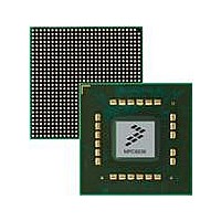
MPC8536DS Freescale Semiconductor, MPC8536DS Datasheet - Page 1680

MPC8536DS
Manufacturer Part Number
MPC8536DS
Description
BOARD DEV SYSTEM MPC8536E
Manufacturer
Freescale Semiconductor
Series
PowerQUICC III™r
Type
MPUr
Datasheets
1.MPC8536EBVTAVLA.pdf
(127 pages)
2.MPC8536EBVTAVLA.pdf
(1706 pages)
3.MPC8536DS.pdf
(2 pages)
4.MPC8536DS.pdf
(126 pages)
Specifications of MPC8536DS
Contents
Board, Software and Documentation
Processor Series
MPC85xx
Core
e500
Data Bus Width
32 bit
Maximum Clock Frequency
667 MHz
Operating Supply Voltage
- 0.3 V to + 1.21 V
Maximum Operating Temperature
+ 105 C
Data Ram Size
32 KB
Interface Type
SPI, USB
Program Memory Type
DDR2, DDR3, SDRAM
Core Size
32 Bit
Program Memory Size
544KB
Cpu Speed
1.5GHz
Digital Ic Case Style
BGA
No. Of Pins
783
Supply Voltage Range
0.95V To 1.05V
Rohs Compliant
Yes
For Use With/related Products
MPC8536
Lead Free Status / RoHS Status
Lead free / RoHS Compliant
- MPC8536EBVTAVLA PDF datasheet
- MPC8536EBVTAVLA PDF datasheet #2
- MPC8536DS PDF datasheet #3
- MPC8536DS PDF datasheet #4
- Current page: 1680 of 1706
- Download datasheet (15Mb)
K
L
M
Glossary-4
Inbound ATMU windows. Mappings that perform address translation from the external
In-order. An aspect of an operation that adheres to a sequential model. An operation is
Integer unit. An execution unit in the core responsible for executing integer instructions.
Inter-packet gap. The gap between the end of one Ethernet packet and the beginning of
Instruction latency. The total number of clock cycles necessary to execute an instruction
Kill. An operation that causes a
L2 cache. Level-2 cache. See
Latency. The number of clock cycles necessary to execute an instruction and make ready
Least-significant bit (lsb). The bit of least value in an address, register, field, data
Least-significant byte (LSB). The byte of least value in an address, register, data element,
Little-endian. A byte-ordering method in memory where the address n of a word
Local access window. Mapping used to translate a region of memory to a particular target
Media access control (MAC) sublayer. Sublayer that provides a logical connection
Media-independent interface (MII) sublayer. Sublayer that provides a standard
MPC83536E PowerQUICC™ III Integrated Processor Reference Manual, Rev. 1
address space to the local address space, attach attributes and transaction types to
the transaction, and map the transaction to its target interface.
said to be performed in-order if, at the time that it is performed, it is known to be
required by the sequential execution model.
the next transmitted packet.
and make ready the results of that instruction.
data to memory.
the results of that execution for a subsequent instruction.
element, or instruction encoding.
or instruction encoding.
corresponds to the least-significant byte. In an addressed memory word, the bytes
are ordered (left to right) 3, 2, 1, 0, with 3 being the most-significant byte. See
Big-endian.
interface, such as the DDR SDRAM controller or the PCI controller. The local
memory map is defined by a set of eight local access windows. The size of each
window can be configured from 4 Kbytes to 2 Gbytes.
between the MAC and its peer station. Its primary responsibility is to initialize,
control, and manage the connection with the peer station.
interface between the MAC layer and the physical layer for 10/100-Mbps
operations. It isolates the MAC layer and the physical layer, enabling the MAC
layer to be used with various implementations of the physical layer.
Secondary
cache block
cache.
to be invalidated without writing any modified
Freescale Semiconductor
Related parts for MPC8536DS
Image
Part Number
Description
Manufacturer
Datasheet
Request
R
Part Number:
Description:
Manufacturer:
Freescale Semiconductor, Inc
Datasheet:
Part Number:
Description:
Manufacturer:
Freescale Semiconductor, Inc
Datasheet:
Part Number:
Description:
Manufacturer:
Freescale Semiconductor, Inc
Datasheet:
Part Number:
Description:
Manufacturer:
Freescale Semiconductor, Inc
Datasheet:
Part Number:
Description:
Manufacturer:
Freescale Semiconductor, Inc
Datasheet:
Part Number:
Description:
Manufacturer:
Freescale Semiconductor, Inc
Datasheet:
Part Number:
Description:
Manufacturer:
Freescale Semiconductor, Inc
Datasheet:
Part Number:
Description:
Manufacturer:
Freescale Semiconductor, Inc
Datasheet:
Part Number:
Description:
Manufacturer:
Freescale Semiconductor, Inc
Datasheet:
Part Number:
Description:
Manufacturer:
Freescale Semiconductor, Inc
Datasheet:
Part Number:
Description:
Manufacturer:
Freescale Semiconductor, Inc
Datasheet:
Part Number:
Description:
Manufacturer:
Freescale Semiconductor, Inc
Datasheet:
Part Number:
Description:
Manufacturer:
Freescale Semiconductor, Inc
Datasheet:
Part Number:
Description:
Manufacturer:
Freescale Semiconductor, Inc
Datasheet:
Part Number:
Description:
Manufacturer:
Freescale Semiconductor, Inc
Datasheet:


