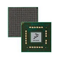
MPC8536DS Freescale Semiconductor, MPC8536DS Datasheet - Page 1340

MPC8536DS
Manufacturer Part Number
MPC8536DS
Description
BOARD DEV SYSTEM MPC8536E
Manufacturer
Freescale Semiconductor
Series
PowerQUICC III™r
Type
MPUr
Datasheets
1.MPC8536EBVTAVLA.pdf
(127 pages)
2.MPC8536EBVTAVLA.pdf
(1706 pages)
3.MPC8536DS.pdf
(2 pages)
4.MPC8536DS.pdf
(126 pages)
Specifications of MPC8536DS
Contents
Board, Software and Documentation
Processor Series
MPC85xx
Core
e500
Data Bus Width
32 bit
Maximum Clock Frequency
667 MHz
Operating Supply Voltage
- 0.3 V to + 1.21 V
Maximum Operating Temperature
+ 105 C
Data Ram Size
32 KB
Interface Type
SPI, USB
Program Memory Type
DDR2, DDR3, SDRAM
Core Size
32 Bit
Program Memory Size
544KB
Cpu Speed
1.5GHz
Digital Ic Case Style
BGA
No. Of Pins
783
Supply Voltage Range
0.95V To 1.05V
Rohs Compliant
Yes
For Use With/related Products
MPC8536
Lead Free Status / RoHS Status
Lead free / RoHS Compliant
- MPC8536EBVTAVLA PDF datasheet
- MPC8536EBVTAVLA PDF datasheet #2
- MPC8536DS PDF datasheet #3
- MPC8536DS PDF datasheet #4
- Current page: 1340 of 1706
- Download datasheet (15Mb)
Universal Serial Bus Interfaces
The following sections provide details about the registers in the USB memory map.
21.3.1
The capability registers specify the software limits, restrictions, and capabilities of the host/device
controller implementation. Most of these registers are defined by the EHCI specification. Registers that
are not defined by the EHCI specification are noted in their descriptions.
21-6
0x000–
0x000–
0xFFC
0xFFC
Offset
Capability Registers
Memory may be viewed from either a big-endian or little-endian byte
ordering perspective depending on the processor configuration. In
big-endian mode, the most-significant byte of word 0 is located at address 0
and the least-significant byte of word 0 is located at address 3. In
little-endian mode, the least-significant byte of word 0 is located at address
0 and the most-significant byte of word 0 is located at address 3. Within
registers, bits are numbered within a word starting with bit 31 as the
most-significant bit. By convention USB registers use little-endian byte
ordering. In the USB module, these are the registers from offsets 0x00 to
0x1FF. The registers associated with the internal system interface (0x400
and above) use big-endian byte ordering.
USB controller 2 registers
Note: All registers defined for USB controller 1 are also defined for USB controller 2; the offsets of USB
USB controller 3 registers
Note: All registers defined for USB controller 1 are also defined for USB controller 3; the offsets of USB
MPC8536E PowerQUICC III Integrated Processor Reference Manual, Rev. 1
controller 2 registers are the same except they have a different block base address.
controller 3 registers are the same except they have a different block base address.
Table 21-2. USB Interface Memory Map (continued)
USB Controller 3—Block Base Address 0x2_B000
USB Controller 1—Block Base Address 0x2_2000
USB Controller 2—Block Base Address 0x2_3000
Register
USB Controller 3 Registers
NOTE
Access
Reset
Freescale Semiconductor
Section/Page
Related parts for MPC8536DS
Image
Part Number
Description
Manufacturer
Datasheet
Request
R
Part Number:
Description:
Manufacturer:
Freescale Semiconductor, Inc
Datasheet:
Part Number:
Description:
Manufacturer:
Freescale Semiconductor, Inc
Datasheet:
Part Number:
Description:
Manufacturer:
Freescale Semiconductor, Inc
Datasheet:
Part Number:
Description:
Manufacturer:
Freescale Semiconductor, Inc
Datasheet:
Part Number:
Description:
Manufacturer:
Freescale Semiconductor, Inc
Datasheet:
Part Number:
Description:
Manufacturer:
Freescale Semiconductor, Inc
Datasheet:
Part Number:
Description:
Manufacturer:
Freescale Semiconductor, Inc
Datasheet:
Part Number:
Description:
Manufacturer:
Freescale Semiconductor, Inc
Datasheet:
Part Number:
Description:
Manufacturer:
Freescale Semiconductor, Inc
Datasheet:
Part Number:
Description:
Manufacturer:
Freescale Semiconductor, Inc
Datasheet:
Part Number:
Description:
Manufacturer:
Freescale Semiconductor, Inc
Datasheet:
Part Number:
Description:
Manufacturer:
Freescale Semiconductor, Inc
Datasheet:
Part Number:
Description:
Manufacturer:
Freescale Semiconductor, Inc
Datasheet:
Part Number:
Description:
Manufacturer:
Freescale Semiconductor, Inc
Datasheet:
Part Number:
Description:
Manufacturer:
Freescale Semiconductor, Inc
Datasheet:


