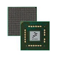
MPC8536DS Freescale Semiconductor, MPC8536DS Datasheet - Page 715

MPC8536DS
Manufacturer Part Number
MPC8536DS
Description
BOARD DEV SYSTEM MPC8536E
Manufacturer
Freescale Semiconductor
Series
PowerQUICC III™r
Type
MPUr
Datasheets
1.MPC8536EBVTAVLA.pdf
(127 pages)
2.MPC8536EBVTAVLA.pdf
(1706 pages)
3.MPC8536DS.pdf
(2 pages)
4.MPC8536DS.pdf
(126 pages)
Specifications of MPC8536DS
Contents
Board, Software and Documentation
Processor Series
MPC85xx
Core
e500
Data Bus Width
32 bit
Maximum Clock Frequency
667 MHz
Operating Supply Voltage
- 0.3 V to + 1.21 V
Maximum Operating Temperature
+ 105 C
Data Ram Size
32 KB
Interface Type
SPI, USB
Program Memory Type
DDR2, DDR3, SDRAM
Core Size
32 Bit
Program Memory Size
544KB
Cpu Speed
1.5GHz
Digital Ic Case Style
BGA
No. Of Pins
783
Supply Voltage Range
0.95V To 1.05V
Rohs Compliant
Yes
For Use With/related Products
MPC8536
Lead Free Status / RoHS Status
Lead free / RoHS Compliant
- MPC8536EBVTAVLA PDF datasheet
- MPC8536EBVTAVLA PDF datasheet #2
- MPC8536DS PDF datasheet #3
- MPC8536DS PDF datasheet #4
- Current page: 715 of 1706
- Download datasheet (15Mb)
13.4.3.4.2
If FCM is selected as the boot ROM controller from power-on-reset configuration, eLBC will
automatically load from bank 0 a single 4 Kbyte page of boot code into the FCM buffer RAM during
HRESET (See
FCM buffer RAM, but must ensure that any further data read from the NAND Flash EEPROM is
transferred under software control in order to continue the bootstrap process.
Since OR0[AM] is initially cleared during reset, all CPU fetches to eLBC will access the FCM buffer
RAM, which appears in the memory map as a 4-Kbyte RAM. No NAND Flash spare regions are mapped
during boot, therefore only 4 Kbytes of contiguous, main region data, loaded from the first pages of the
boot block, are accessible in eLBC bank 0, as indicated in
The process for booting is as follows:
Freescale Semiconductor
1. Following negation of HRESET, eLBC is released from reset and commences automatic boot
2. FCM starts searching for a valid boot block at block index 0.
block loading if FCM is selected as the boot ROM location. Small-page or large-page, 8-bit NAND
Flash devices can be used for boot loading when enabled with LCS0. eLBC drives LFWP low
during boot accesses to prevent accidental erasure of the NAND Flash boot ROM.
Table 13-38. Boot Bank Field Values after Reset for FCM as Boot Controller (continued)
Section 4.4.3.6, “Boot ROM
Boot Block Loading into the FCM Buffer RAM
Register
MPC8536E PowerQUICC III Integrated Processor Reference Manual, Rev. 1
OR0
Figure 13-60. FCM Buffer RAM Memory Map During Boot Loading
Bank Base Address
offset 0x1000
End of Bank
BCTLD
CSCT
EHTR
TRLX
Field
PGS
CHT
SCY
CST
RST
AM
boot block buffer
replicated FCM
buffer RAM
images in bank
Location.”). The CPU can execute boot code directly from the
0000_0000_0000_0000_0
From por_cfg_scy[1:3]
From cfg_rom_loc
Figure
4096-byte boot block
—no NAND Flash spare regions
Setting
0
1
1
1
1
1
1
13-60.
Enhanced Local Bus Controller
13-73
Related parts for MPC8536DS
Image
Part Number
Description
Manufacturer
Datasheet
Request
R
Part Number:
Description:
Manufacturer:
Freescale Semiconductor, Inc
Datasheet:
Part Number:
Description:
Manufacturer:
Freescale Semiconductor, Inc
Datasheet:
Part Number:
Description:
Manufacturer:
Freescale Semiconductor, Inc
Datasheet:
Part Number:
Description:
Manufacturer:
Freescale Semiconductor, Inc
Datasheet:
Part Number:
Description:
Manufacturer:
Freescale Semiconductor, Inc
Datasheet:
Part Number:
Description:
Manufacturer:
Freescale Semiconductor, Inc
Datasheet:
Part Number:
Description:
Manufacturer:
Freescale Semiconductor, Inc
Datasheet:
Part Number:
Description:
Manufacturer:
Freescale Semiconductor, Inc
Datasheet:
Part Number:
Description:
Manufacturer:
Freescale Semiconductor, Inc
Datasheet:
Part Number:
Description:
Manufacturer:
Freescale Semiconductor, Inc
Datasheet:
Part Number:
Description:
Manufacturer:
Freescale Semiconductor, Inc
Datasheet:
Part Number:
Description:
Manufacturer:
Freescale Semiconductor, Inc
Datasheet:
Part Number:
Description:
Manufacturer:
Freescale Semiconductor, Inc
Datasheet:
Part Number:
Description:
Manufacturer:
Freescale Semiconductor, Inc
Datasheet:
Part Number:
Description:
Manufacturer:
Freescale Semiconductor, Inc
Datasheet:


