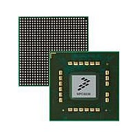
MPC8536DS Freescale Semiconductor, MPC8536DS Datasheet - Page 684

MPC8536DS
Manufacturer Part Number
MPC8536DS
Description
BOARD DEV SYSTEM MPC8536E
Manufacturer
Freescale Semiconductor
Series
PowerQUICC III™r
Type
MPUr
Datasheets
1.MPC8536EBVTAVLA.pdf
(127 pages)
2.MPC8536EBVTAVLA.pdf
(1706 pages)
3.MPC8536DS.pdf
(2 pages)
4.MPC8536DS.pdf
(126 pages)
Specifications of MPC8536DS
Contents
Board, Software and Documentation
Processor Series
MPC85xx
Core
e500
Data Bus Width
32 bit
Maximum Clock Frequency
667 MHz
Operating Supply Voltage
- 0.3 V to + 1.21 V
Maximum Operating Temperature
+ 105 C
Data Ram Size
32 KB
Interface Type
SPI, USB
Program Memory Type
DDR2, DDR3, SDRAM
Core Size
32 Bit
Program Memory Size
544KB
Cpu Speed
1.5GHz
Digital Ic Case Style
BGA
No. Of Pins
783
Supply Voltage Range
0.95V To 1.05V
Rohs Compliant
Yes
For Use With/related Products
MPC8536
Lead Free Status / RoHS Status
Lead free / RoHS Compliant
- MPC8536EBVTAVLA PDF datasheet
- MPC8536EBVTAVLA PDF datasheet #2
- MPC8536DS PDF datasheet #3
- MPC8536DS PDF datasheet #4
- Current page: 684 of 1706
- Download datasheet (15Mb)
Enhanced Local Bus Controller
13.4
The eLBC allows the implementation of memory systems with very specific timing requirements.
13-42
8–31
Bits
•
•
•
1–7
0
The GPCM provides interfacing for simpler, lower-performance memories and memory-mapped
devices. It has inherently lower performance because it does not support bursting. For this reason,
GPCM-controlled banks are used primarily for boot-loading from NVRAM or NOR Flash, and
access to low-performance memory-mapped peripherals.
The FCM interfaces the eLBC to NAND Flash EEPROMs with 8-bit data bus. The FCM has an
automatic boot-loading feature that allows the CPU to boot from high density EEPROM, loading
the boot block into 4 Kbytes of RAM for execution of the first level boot code. Following boot,
FCM provides a flexible instruction sequencer that allows a user-defined command, address, and
data transfer sequence of up to 8 steps to be executed against a memory-mapped buffer RAM.
Programmable set-up time, hold time, and wait states permit the FCM to maximize the
performance of NAND Flash block transfers, which can proceed in parallel with software
processing of the multiple RAM buffers. A single-pass ECC engine in the FCM permits
zero-overhead error checking, reporting, and correction in both boot blocks and page data transfers
if enabled.
The UPM supports refresh timers, address multiplexing of the external bus, and generation of
programmable control signals for row address and column address strobes, to allow for a minimal
glue logic interface to DRAMs, burstable SRAMs, and almost any other kind of peripheral with
asynchronous timing or single data rate clocking. The UPM can be used to generate flexible,
user-defined timing patterns for control signals that govern a memory device. These patterns define
how the external control signals behave during a read, write, burst-read, or burst-write access.
Refresh timers are also available to periodically initiate user-defined refresh patterns.
Functional Description
Name
ECC
—
V
Valid bit. This bit denotes that the ECC stored in this register is valid. It is set for full page write/read
transfers if ECC generation/checking is enabled in BR n [DECC].
Reserved
24 bit ECC; For n
page where k = 0,1,2,...). It stores calculated ECC value during writes/reads.
MPC8536E PowerQUICC III Integrated Processor Reference Manual, Rev. 1
th
Table 13-31. FECC n Field Descriptions
512 bytes of a page in case of large page or for (4 k + n)
Description
th
512 byte page for small
Freescale Semiconductor
Related parts for MPC8536DS
Image
Part Number
Description
Manufacturer
Datasheet
Request
R
Part Number:
Description:
Manufacturer:
Freescale Semiconductor, Inc
Datasheet:
Part Number:
Description:
Manufacturer:
Freescale Semiconductor, Inc
Datasheet:
Part Number:
Description:
Manufacturer:
Freescale Semiconductor, Inc
Datasheet:
Part Number:
Description:
Manufacturer:
Freescale Semiconductor, Inc
Datasheet:
Part Number:
Description:
Manufacturer:
Freescale Semiconductor, Inc
Datasheet:
Part Number:
Description:
Manufacturer:
Freescale Semiconductor, Inc
Datasheet:
Part Number:
Description:
Manufacturer:
Freescale Semiconductor, Inc
Datasheet:
Part Number:
Description:
Manufacturer:
Freescale Semiconductor, Inc
Datasheet:
Part Number:
Description:
Manufacturer:
Freescale Semiconductor, Inc
Datasheet:
Part Number:
Description:
Manufacturer:
Freescale Semiconductor, Inc
Datasheet:
Part Number:
Description:
Manufacturer:
Freescale Semiconductor, Inc
Datasheet:
Part Number:
Description:
Manufacturer:
Freescale Semiconductor, Inc
Datasheet:
Part Number:
Description:
Manufacturer:
Freescale Semiconductor, Inc
Datasheet:
Part Number:
Description:
Manufacturer:
Freescale Semiconductor, Inc
Datasheet:
Part Number:
Description:
Manufacturer:
Freescale Semiconductor, Inc
Datasheet:


