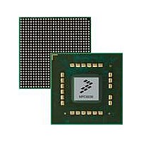
MPC8536DS Freescale Semiconductor, MPC8536DS Datasheet - Page 335

MPC8536DS
Manufacturer Part Number
MPC8536DS
Description
BOARD DEV SYSTEM MPC8536E
Manufacturer
Freescale Semiconductor
Series
PowerQUICC III™r
Type
MPUr
Datasheets
1.MPC8536EBVTAVLA.pdf
(127 pages)
2.MPC8536EBVTAVLA.pdf
(1706 pages)
3.MPC8536DS.pdf
(2 pages)
4.MPC8536DS.pdf
(126 pages)
Specifications of MPC8536DS
Contents
Board, Software and Documentation
Processor Series
MPC85xx
Core
e500
Data Bus Width
32 bit
Maximum Clock Frequency
667 MHz
Operating Supply Voltage
- 0.3 V to + 1.21 V
Maximum Operating Temperature
+ 105 C
Data Ram Size
32 KB
Interface Type
SPI, USB
Program Memory Type
DDR2, DDR3, SDRAM
Core Size
32 Bit
Program Memory Size
544KB
Cpu Speed
1.5GHz
Digital Ic Case Style
BGA
No. Of Pins
783
Supply Voltage Range
0.95V To 1.05V
Rohs Compliant
Yes
For Use With/related Products
MPC8536
Lead Free Status / RoHS Status
Lead free / RoHS Compliant
- MPC8536EBVTAVLA PDF datasheet
- MPC8536EBVTAVLA PDF datasheet #2
- MPC8536DS PDF datasheet #3
- MPC8536DS PDF datasheet #4
- Current page: 335 of 1706
- Download datasheet (15Mb)
Read and write accesses to memory are burst oriented; accesses start at a selected location and continue
for a programmed number of higher locations (4 or 8) in a programmed sequence. Accesses to closed pages
start with the registration of an ACTIVE command followed by a READ or WRITE. (Accessing open
pages does not require an ACTIVE command.) The address bits registered coincident with the activate
command specifies the logical bank and row to be accessed. The address coincident with the READ or
WRITE command specify the logical bank and starting column for the burst access.
The data interface is source synchronous, meaning whatever sources the data also provides a clocking
signal to synchronize data reception. These bidirectional data strobes (MDQS[0:8]) are inputs to the
controller during reads and outputs during writes. The DDR SDRAM specification requires the data strobe
signals to be centered within the data tenure during writes and to be offset by the controller to the center
of the data tenure during reads. This delay is implemented in the controller for both reads and writes.
When ECC is enabled, 1 clock cycle is added to the read path to check ECC and correct single-bit errors.
ECC generation does not add a cycle to the write path.
Freescale Semiconductor
Request from
Address from
Management
Data from
Data from
SDRAM
To Error
ECM
Master
Master
Master
MPC8536E PowerQUICC III Integrated Processor Reference Manual, Rev. 1
DQ
Signals
Error
Address
Decode
RMW
Figure 8-45. DDR Memory Controller Block Diagram
ECC
DQ
Open
Table
Row
ECC
Delay Chain
DQ
FIFO
FIFO
NEG
POS
Address
SDRAM
Control
Control
SDRAM
Control
EN
EN
DDR SDRAM
Memory Array
DDR SDRAM
Memory Control
Data Strobes
Data Signals
Clocks
Debug Signals
MA[15:0]
MBA[2:0]
MSRCID[0:4]
MDVAL
MCS[0:3]
MCAS
MRAS
MWE
MDM[0:8]
MCKE[0:3]
MODT[0:3]
MDQS[0:8]
MDQS[0:8]
MDQ[0:63]
MECC[0:7]
MCK[0:5]
MCK[0:5]
DDR Memory Controller
8-61
Related parts for MPC8536DS
Image
Part Number
Description
Manufacturer
Datasheet
Request
R
Part Number:
Description:
Manufacturer:
Freescale Semiconductor, Inc
Datasheet:
Part Number:
Description:
Manufacturer:
Freescale Semiconductor, Inc
Datasheet:
Part Number:
Description:
Manufacturer:
Freescale Semiconductor, Inc
Datasheet:
Part Number:
Description:
Manufacturer:
Freescale Semiconductor, Inc
Datasheet:
Part Number:
Description:
Manufacturer:
Freescale Semiconductor, Inc
Datasheet:
Part Number:
Description:
Manufacturer:
Freescale Semiconductor, Inc
Datasheet:
Part Number:
Description:
Manufacturer:
Freescale Semiconductor, Inc
Datasheet:
Part Number:
Description:
Manufacturer:
Freescale Semiconductor, Inc
Datasheet:
Part Number:
Description:
Manufacturer:
Freescale Semiconductor, Inc
Datasheet:
Part Number:
Description:
Manufacturer:
Freescale Semiconductor, Inc
Datasheet:
Part Number:
Description:
Manufacturer:
Freescale Semiconductor, Inc
Datasheet:
Part Number:
Description:
Manufacturer:
Freescale Semiconductor, Inc
Datasheet:
Part Number:
Description:
Manufacturer:
Freescale Semiconductor, Inc
Datasheet:
Part Number:
Description:
Manufacturer:
Freescale Semiconductor, Inc
Datasheet:
Part Number:
Description:
Manufacturer:
Freescale Semiconductor, Inc
Datasheet:


