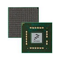
MPC8536DS Freescale Semiconductor, MPC8536DS Datasheet - Page 763

MPC8536DS
Manufacturer Part Number
MPC8536DS
Description
BOARD DEV SYSTEM MPC8536E
Manufacturer
Freescale Semiconductor
Series
PowerQUICC III™r
Type
MPUr
Datasheets
1.MPC8536EBVTAVLA.pdf
(127 pages)
2.MPC8536EBVTAVLA.pdf
(1706 pages)
3.MPC8536DS.pdf
(2 pages)
4.MPC8536DS.pdf
(126 pages)
Specifications of MPC8536DS
Contents
Board, Software and Documentation
Processor Series
MPC85xx
Core
e500
Data Bus Width
32 bit
Maximum Clock Frequency
667 MHz
Operating Supply Voltage
- 0.3 V to + 1.21 V
Maximum Operating Temperature
+ 105 C
Data Ram Size
32 KB
Interface Type
SPI, USB
Program Memory Type
DDR2, DDR3, SDRAM
Core Size
32 Bit
Program Memory Size
544KB
Cpu Speed
1.5GHz
Digital Ic Case Style
BGA
No. Of Pins
783
Supply Voltage Range
0.95V To 1.05V
Rohs Compliant
Yes
For Use With/related Products
MPC8536
Lead Free Status / RoHS Status
Lead free / RoHS Compliant
- MPC8536EBVTAVLA PDF datasheet
- MPC8536EBVTAVLA PDF datasheet #2
- MPC8536DS PDF datasheet #3
- MPC8536DS PDF datasheet #4
- Current page: 763 of 1706
- Download datasheet (15Mb)
14.5.1
Each of the eTSECs is allocated 4 Kbytes of memory-mapped space. The space for each eTSEC is divided
as indicated in
14.5.2
The eTSEC memory mapped registers are accessed by reading and writing to an address comprised of the
base address (specified in CCSRBAR as defined in
address, plus the offset of the specific register to be accessed. Note that all memory-mapped registers must
only be accessed as 32-bit quantities.
Table 14-4
offsets to the memory map table are applicable to each eTSEC. Block base addresses are as follows:
In this table and in the register figures and field descriptions, the following access definitions apply:
Freescale Semiconductor
•
•
•
•
•
•
•
eTSEC1 starts at 0x2_4000 address offset
eTSEC3 starts at 0x2_6000 address offset
Reserved fields are always ignored for the purposes of determining access type.
R/W, R, and W (read/write, read only, and write only) indicate that all the non-reserved fields in a
register have the same access type.
w1c indicates that all of the non-reserved fields in a register are cleared by writing ones to them.
Mixed indicates a combination of access types.
Special is used when no other category applies. In this case the register figure and field description
table should be read carefully.
lists the offset, name, and a cross-reference to the complete description of each register. The
Top-Level Module Memory Map
Detailed Memory Map
Table
MPC8536E PowerQUICC III Integrated Processor Reference Manual, Rev. 1
14-3.
Address Offset
C00–C3F
C40–DFF
A00–AFF
B00–BFF
E00–EFF
000–0FF
100–2FF
300–4FF
500–5FF
600–7FF
800–8FF
900–9FF
Table 14-3. Module Memory Map Summary
eTSEC general control/status registers
eTSEC transmit control/status registers
eTSEC receive control/status registers
MAC registers
RMON MIB registers
Hash table registers
FIFO control/status registers
DMA system registers
Lossless Flow Control registers
1588 Hardware Assist
Chapter 2, “Memory
Function
—
—
Enhanced Three-Speed Ethernet Controllers
Map.”) plus the block base
14-15
Related parts for MPC8536DS
Image
Part Number
Description
Manufacturer
Datasheet
Request
R
Part Number:
Description:
Manufacturer:
Freescale Semiconductor, Inc
Datasheet:
Part Number:
Description:
Manufacturer:
Freescale Semiconductor, Inc
Datasheet:
Part Number:
Description:
Manufacturer:
Freescale Semiconductor, Inc
Datasheet:
Part Number:
Description:
Manufacturer:
Freescale Semiconductor, Inc
Datasheet:
Part Number:
Description:
Manufacturer:
Freescale Semiconductor, Inc
Datasheet:
Part Number:
Description:
Manufacturer:
Freescale Semiconductor, Inc
Datasheet:
Part Number:
Description:
Manufacturer:
Freescale Semiconductor, Inc
Datasheet:
Part Number:
Description:
Manufacturer:
Freescale Semiconductor, Inc
Datasheet:
Part Number:
Description:
Manufacturer:
Freescale Semiconductor, Inc
Datasheet:
Part Number:
Description:
Manufacturer:
Freescale Semiconductor, Inc
Datasheet:
Part Number:
Description:
Manufacturer:
Freescale Semiconductor, Inc
Datasheet:
Part Number:
Description:
Manufacturer:
Freescale Semiconductor, Inc
Datasheet:
Part Number:
Description:
Manufacturer:
Freescale Semiconductor, Inc
Datasheet:
Part Number:
Description:
Manufacturer:
Freescale Semiconductor, Inc
Datasheet:
Part Number:
Description:
Manufacturer:
Freescale Semiconductor, Inc
Datasheet:


