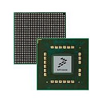
MPC8536DS Freescale Semiconductor, MPC8536DS Datasheet - Page 638

MPC8536DS
Manufacturer Part Number
MPC8536DS
Description
BOARD DEV SYSTEM MPC8536E
Manufacturer
Freescale Semiconductor
Series
PowerQUICC III™r
Type
MPUr
Datasheets
1.MPC8536EBVTAVLA.pdf
(127 pages)
2.MPC8536EBVTAVLA.pdf
(1706 pages)
3.MPC8536DS.pdf
(2 pages)
4.MPC8536DS.pdf
(126 pages)
Specifications of MPC8536DS
Contents
Board, Software and Documentation
Processor Series
MPC85xx
Core
e500
Data Bus Width
32 bit
Maximum Clock Frequency
667 MHz
Operating Supply Voltage
- 0.3 V to + 1.21 V
Maximum Operating Temperature
+ 105 C
Data Ram Size
32 KB
Interface Type
SPI, USB
Program Memory Type
DDR2, DDR3, SDRAM
Core Size
32 Bit
Program Memory Size
544KB
Cpu Speed
1.5GHz
Digital Ic Case Style
BGA
No. Of Pins
783
Supply Voltage Range
0.95V To 1.05V
Rohs Compliant
Yes
For Use With/related Products
MPC8536
Lead Free Status / RoHS Status
Lead free / RoHS Compliant
- MPC8536EBVTAVLA PDF datasheet
- MPC8536EBVTAVLA PDF datasheet #2
- MPC8536DS PDF datasheet #3
- MPC8536DS PDF datasheet #4
- Current page: 638 of 1706
- Download datasheet (15Mb)
DUART
A standard UART bus transfer is composed of either three or four parts:
An internal logic sample signal, rxcnt, uses the frequency of the baud-rate generator to drive the bits on
SOUT.
The following sections describe the four components of the serial interface, the baud-rate generator, local
loopback mode, different errors, and FIFO mode.
12.4.1.1
A write to the transmitter holding register (UTHR) generates a START bit on the SOUT signal.
Figure 12-16
new data transfer which is limited to the bit length programmed in the UART line control register
(ULCR).When the bus is idle, SOUT is high.
12.4.1.2
Each data transfer contains 5–8 bits of data. The ULCR data bit length for the transmitter and receiver
UART devices must agree before a transfer begins; otherwise, a parity or framing error may occur. A
transfer begins when UTHR is written. At that time a START bit is generated followed by 5–8 of the data
bits previously written to the UTHR. The data bits are driven from the least significant to the most
significant bits. After the parity and STOP bits, a new data transfer can begin if new data is written to the
UTHR.
12.4.1.3
The user has the option of using even, odd, no parity, or stick parity (see
Registers (ULCRn).”
transfer data. When receiving data a parity error can occur if an unexpected parity value is detected. (See
Section 12.3.1.10, “Line Status Registers
12.4.1.4
The transmitter device ends the write transfer by generating a STOP bit. The STOP bit is always high. The
user can program the length of the STOP bit(s) in the ULCR. Both the receiver and transmitter STOP bit
length must agree before attempting to transfer data. A framing error can occur if an invalid STOP bit is
detected.
12.4.2
Each UART contains an independent programmable baud-rate generator, that is capable of taking the
platform clock input and dividing the input by any divisor from 1 to 2
12-20
•
•
•
•
START bit
Data transfer bits (least-significant bit is first data bit on the bus)
Parity bit (optional)
STOP bits
Baud-Rate Generator Logic
shows that the START bit is defined as a logic 0. The START bit denotes the beginning of a
START Bit
Data Transfer
Parity Bit
STOP Bit
MPC8536E PowerQUICC III Integrated Processor Reference Manual, Rev. 1
Both the receiver and transmitter parity definition must agree before attempting to
(ULSRn).”)
16
– 1.
Section 12.3.1.8, “Line Control
Freescale Semiconductor
Related parts for MPC8536DS
Image
Part Number
Description
Manufacturer
Datasheet
Request
R
Part Number:
Description:
Manufacturer:
Freescale Semiconductor, Inc
Datasheet:
Part Number:
Description:
Manufacturer:
Freescale Semiconductor, Inc
Datasheet:
Part Number:
Description:
Manufacturer:
Freescale Semiconductor, Inc
Datasheet:
Part Number:
Description:
Manufacturer:
Freescale Semiconductor, Inc
Datasheet:
Part Number:
Description:
Manufacturer:
Freescale Semiconductor, Inc
Datasheet:
Part Number:
Description:
Manufacturer:
Freescale Semiconductor, Inc
Datasheet:
Part Number:
Description:
Manufacturer:
Freescale Semiconductor, Inc
Datasheet:
Part Number:
Description:
Manufacturer:
Freescale Semiconductor, Inc
Datasheet:
Part Number:
Description:
Manufacturer:
Freescale Semiconductor, Inc
Datasheet:
Part Number:
Description:
Manufacturer:
Freescale Semiconductor, Inc
Datasheet:
Part Number:
Description:
Manufacturer:
Freescale Semiconductor, Inc
Datasheet:
Part Number:
Description:
Manufacturer:
Freescale Semiconductor, Inc
Datasheet:
Part Number:
Description:
Manufacturer:
Freescale Semiconductor, Inc
Datasheet:
Part Number:
Description:
Manufacturer:
Freescale Semiconductor, Inc
Datasheet:
Part Number:
Description:
Manufacturer:
Freescale Semiconductor, Inc
Datasheet:


