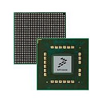
MPC8536DS Freescale Semiconductor, MPC8536DS Datasheet - Page 1076

MPC8536DS
Manufacturer Part Number
MPC8536DS
Description
BOARD DEV SYSTEM MPC8536E
Manufacturer
Freescale Semiconductor
Series
PowerQUICC III™r
Type
MPUr
Datasheets
1.MPC8536EBVTAVLA.pdf
(127 pages)
2.MPC8536EBVTAVLA.pdf
(1706 pages)
3.MPC8536DS.pdf
(2 pages)
4.MPC8536DS.pdf
(126 pages)
Specifications of MPC8536DS
Contents
Board, Software and Documentation
Processor Series
MPC85xx
Core
e500
Data Bus Width
32 bit
Maximum Clock Frequency
667 MHz
Operating Supply Voltage
- 0.3 V to + 1.21 V
Maximum Operating Temperature
+ 105 C
Data Ram Size
32 KB
Interface Type
SPI, USB
Program Memory Type
DDR2, DDR3, SDRAM
Core Size
32 Bit
Program Memory Size
544KB
Cpu Speed
1.5GHz
Digital Ic Case Style
BGA
No. Of Pins
783
Supply Voltage Range
0.95V To 1.05V
Rohs Compliant
Yes
For Use With/related Products
MPC8536
Lead Free Status / RoHS Status
Lead free / RoHS Compliant
- MPC8536EBVTAVLA PDF datasheet
- MPC8536EBVTAVLA PDF datasheet #2
- MPC8536DS PDF datasheet #3
- MPC8536DS PDF datasheet #4
- Current page: 1076 of 1706
- Download datasheet (15Mb)
PCI Bus Interface
16.4.2.7
PCI Bus Transactions
This section provides descriptions of the PCI bus transactions. All bus transactions follow the protocol as
described in
Section 16.4.2, “PCI Bus Protocol.”
Read and write transactions are similar for the memory
and I/O spaces, so they are described as generic read transactions and generic write transactions.
The timing diagrams in this section show the relationship of significant signals involved in bus
transactions. When a signal is drawn as a solid line, it is actively being driven by the current master or
target. When a signal is drawn as a dashed line, no agent is actively driving it. High-impedance signals are
indicated to have indeterminate values when the dashed line is between the two rails.
The terms ‘edge’ and ‘clock edge’ always refer to the rising edge of the clock. The terms ‘asserted’ and
‘negated’ always refer to the globally visible state of the signal on the clock edge, and not to signal
transitions. ‘
’ represents a turnaround cycle in the timing diagrams.
16.4.2.7.1
PCI Read Transactions
This section describes PCI single-beat read transactions and PCI burst read transactions.
A read transaction starts with the address phase, occurring when an initiator asserts PCI_FRAME. During
the address phase, PCI_AD[31:0] contains a valid address and PCI_C/BE[3:0] contains a valid bus
command.
The first data phase of a read transaction requires a turnaround cycle. This allows the transition from the
initiator driving PCI_AD[31:0] as address signals to the target driving PCI_AD[31:0] as data signals. The
turnaround cycle is enforced by the target with the TRDY signal. The target provides valid data at the
earliest one cycle after the turnaround cycle. The target must drive the PCI_AD[31:0] signals when
PCI_DEVSEL is asserted.
During the data phase, the PCI_C/BE[3:0] signals indicate which byte lanes are involved in the current
data phase. A data phase may consist of a data transfer and wait cycles. The PCI_C/BE[3:0] signals remain
actively driven for both reads and writes from the first clock of the data phase through the end of the
transaction.
A data phase completes when data is transferred, which occurs when both PCI_IRDY and PCI_TRDY are
asserted on the same clock edge. When either PCI_IRDY or PCI_TRDY is negated, a wait cycle is inserted
and no data is transferred. The initiator indicates the last data phase by negating PCI_FRAME when
PCI_IRDY is asserted. The transaction is considered complete when data is transferred in the last data
phase.
MPC8536E PowerQUICC III Integrated Processor Reference Manual, Rev. 1
16-50
Freescale Semiconductor
Related parts for MPC8536DS
Image
Part Number
Description
Manufacturer
Datasheet
Request
R
Part Number:
Description:
Manufacturer:
Freescale Semiconductor, Inc
Datasheet:
Part Number:
Description:
Manufacturer:
Freescale Semiconductor, Inc
Datasheet:
Part Number:
Description:
Manufacturer:
Freescale Semiconductor, Inc
Datasheet:
Part Number:
Description:
Manufacturer:
Freescale Semiconductor, Inc
Datasheet:
Part Number:
Description:
Manufacturer:
Freescale Semiconductor, Inc
Datasheet:
Part Number:
Description:
Manufacturer:
Freescale Semiconductor, Inc
Datasheet:
Part Number:
Description:
Manufacturer:
Freescale Semiconductor, Inc
Datasheet:
Part Number:
Description:
Manufacturer:
Freescale Semiconductor, Inc
Datasheet:
Part Number:
Description:
Manufacturer:
Freescale Semiconductor, Inc
Datasheet:
Part Number:
Description:
Manufacturer:
Freescale Semiconductor, Inc
Datasheet:
Part Number:
Description:
Manufacturer:
Freescale Semiconductor, Inc
Datasheet:
Part Number:
Description:
Manufacturer:
Freescale Semiconductor, Inc
Datasheet:
Part Number:
Description:
Manufacturer:
Freescale Semiconductor, Inc
Datasheet:
Part Number:
Description:
Manufacturer:
Freescale Semiconductor, Inc
Datasheet:
Part Number:
Description:
Manufacturer:
Freescale Semiconductor, Inc
Datasheet:


