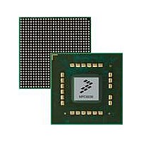
MPC8536DS Freescale Semiconductor, MPC8536DS Datasheet - Page 680

MPC8536DS
Manufacturer Part Number
MPC8536DS
Description
BOARD DEV SYSTEM MPC8536E
Manufacturer
Freescale Semiconductor
Series
PowerQUICC III™r
Type
MPUr
Datasheets
1.MPC8536EBVTAVLA.pdf
(127 pages)
2.MPC8536EBVTAVLA.pdf
(1706 pages)
3.MPC8536DS.pdf
(2 pages)
4.MPC8536DS.pdf
(126 pages)
Specifications of MPC8536DS
Contents
Board, Software and Documentation
Processor Series
MPC85xx
Core
e500
Data Bus Width
32 bit
Maximum Clock Frequency
667 MHz
Operating Supply Voltage
- 0.3 V to + 1.21 V
Maximum Operating Temperature
+ 105 C
Data Ram Size
32 KB
Interface Type
SPI, USB
Program Memory Type
DDR2, DDR3, SDRAM
Core Size
32 Bit
Program Memory Size
544KB
Cpu Speed
1.5GHz
Digital Ic Case Style
BGA
No. Of Pins
783
Supply Voltage Range
0.95V To 1.05V
Rohs Compliant
Yes
For Use With/related Products
MPC8536
Lead Free Status / RoHS Status
Lead free / RoHS Compliant
- MPC8536EBVTAVLA PDF datasheet
- MPC8536EBVTAVLA PDF datasheet #2
- MPC8536DS PDF datasheet #3
- MPC8536DS PDF datasheet #4
- Current page: 680 of 1706
- Download datasheet (15Mb)
Enhanced Local Bus Controller
Table 13-25
13.3.1.19 Flash Command Register (FCR)
The local bus Flash command register (FCR), shown in
EEPROM command bytes that may be referenced by opcodes in FIR during FCM operation. The values
of the commands should follow the manufacturer’s datasheet for the relevant NAND Flash device.
Table 13-26
13-38
Offset 0x0_50E8
Reset
12–15
16–19
20–23
24–27
28–31
16–23
24–31
8–11
8–15
Bits
Bits
0–3
4–7
W
0–7
R
0
CMD0 General purpose FCM Flash command byte 0. Opcodes in FIR that issue command index 0 write
CMD1 General purpose FCM Flash command byte 1. Opcodes in FIR that issue command index 1 write
CMD2 General purpose FCM Flash command byte 2. Opcodes in FIR that issue command index 2 write
CMD3 General purpose FCM Flash command byte 3. Opcodes in FIR that issue command index 3 write
Name
Name
OP0
OP1
OP2
OP3
OP4
OP5
OP6
OP7
describes FIR fields.
describes FCR fields.
CMD0
FCM operation codes. OP0 is executed first, followed by OP1, through to OP7.
0000 NOP—No-operation and end of operation sequence
0001 CA—Issue current column address as set in FPAR, with length set by ORx[PGS]
0010 PA—Issue current block+page address as set in FBAR and FPAR, with length set by FMR[AL]
0011 UA—Issue user-defined address byte from next AS field in MDR
0100 CM0—Issue command from FCR[CMD0]
0101 CM1—Issue command from FCR[CMD1]
0110 CM2—Issue command from FCR[CMD2]
0111 CM3—Issue command from FCR[CMD3]
1000 WB—Write FBCR bytes of data from current FCM buffer to Flash device
1001 WS—Write one byte (8b port) of data from next AS field of MDR to Flash device
1010 RB—Read FBCR bytes of data from Flash device into current FCM RAM buffer
1011 RS—Read one byte (8b port) of data from Flash device into next AS field of MDR
1100 CW0—Wait for LFRB to return high or time-out, then issue command from FCR[CMD0]
1101 CW1—Wait for LFRB to return high or time-out, then issue command from FCR[CMD1]
1110 RBW—Wait for LFRB to return high or time-out, then read FBCR bytes of data from Flash device
1111 RSW—Wait for LFRB to return high or time-out, then read one byte (8b port) of data from Flash
CMD0 to the NAND Flash command/data bus.
CMD1 to the NAND Flash command/data bus.
CMD2 to the NAND Flash command/data bus.
CMD3 to the NAND Flash command/data bus.
MPC8536E PowerQUICC III Integrated Processor Reference Manual, Rev. 1
into current FCM RAM buffer
device into next AS field of MDR
7
8
Figure 13-23. Flash Command Register
Table 13-26. FCR Field Descriptions
Table 13-25. FIR Field Descriptions
CMD1
All zeros
15 16
Description
Description
Figure
13-23, holds up to four NAND Flash
CMD2
23 24
Freescale Semiconductor
Access: Read/Write
CMD3
31
Related parts for MPC8536DS
Image
Part Number
Description
Manufacturer
Datasheet
Request
R
Part Number:
Description:
Manufacturer:
Freescale Semiconductor, Inc
Datasheet:
Part Number:
Description:
Manufacturer:
Freescale Semiconductor, Inc
Datasheet:
Part Number:
Description:
Manufacturer:
Freescale Semiconductor, Inc
Datasheet:
Part Number:
Description:
Manufacturer:
Freescale Semiconductor, Inc
Datasheet:
Part Number:
Description:
Manufacturer:
Freescale Semiconductor, Inc
Datasheet:
Part Number:
Description:
Manufacturer:
Freescale Semiconductor, Inc
Datasheet:
Part Number:
Description:
Manufacturer:
Freescale Semiconductor, Inc
Datasheet:
Part Number:
Description:
Manufacturer:
Freescale Semiconductor, Inc
Datasheet:
Part Number:
Description:
Manufacturer:
Freescale Semiconductor, Inc
Datasheet:
Part Number:
Description:
Manufacturer:
Freescale Semiconductor, Inc
Datasheet:
Part Number:
Description:
Manufacturer:
Freescale Semiconductor, Inc
Datasheet:
Part Number:
Description:
Manufacturer:
Freescale Semiconductor, Inc
Datasheet:
Part Number:
Description:
Manufacturer:
Freescale Semiconductor, Inc
Datasheet:
Part Number:
Description:
Manufacturer:
Freescale Semiconductor, Inc
Datasheet:
Part Number:
Description:
Manufacturer:
Freescale Semiconductor, Inc
Datasheet:


