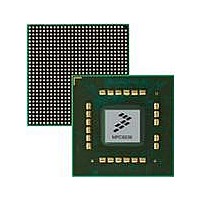
MPC8536DS Freescale Semiconductor, MPC8536DS Datasheet - Page 283

MPC8536DS
Manufacturer Part Number
MPC8536DS
Description
BOARD DEV SYSTEM MPC8536E
Manufacturer
Freescale Semiconductor
Series
PowerQUICC III™r
Type
MPUr
Datasheets
1.MPC8536EBVTAVLA.pdf
(127 pages)
2.MPC8536EBVTAVLA.pdf
(1706 pages)
3.MPC8536DS.pdf
(2 pages)
4.MPC8536DS.pdf
(126 pages)
Specifications of MPC8536DS
Contents
Board, Software and Documentation
Processor Series
MPC85xx
Core
e500
Data Bus Width
32 bit
Maximum Clock Frequency
667 MHz
Operating Supply Voltage
- 0.3 V to + 1.21 V
Maximum Operating Temperature
+ 105 C
Data Ram Size
32 KB
Interface Type
SPI, USB
Program Memory Type
DDR2, DDR3, SDRAM
Core Size
32 Bit
Program Memory Size
544KB
Cpu Speed
1.5GHz
Digital Ic Case Style
BGA
No. Of Pins
783
Supply Voltage Range
0.95V To 1.05V
Rohs Compliant
Yes
For Use With/related Products
MPC8536
Lead Free Status / RoHS Status
Lead free / RoHS Compliant
- MPC8536EBVTAVLA PDF datasheet
- MPC8536EBVTAVLA PDF datasheet #2
- MPC8536DS PDF datasheet #3
- MPC8536DS PDF datasheet #4
- Current page: 283 of 1706
- Download datasheet (15Mb)
Freescale Semiconductor
MODT[0:3]
MDIC[0:1]
MDM[0:8]
MAPAR_
MAPAR_
Signal
ERR
OUT
Table 8-3. Memory Interface Signals—Detailed Signal Descriptions (continued)
I/O
I/O Driver impedance calibration. Note that the MDIC signals require the use of 18.2-
O
O
O
I
MPC8536E PowerQUICC III Integrated Processor Reference Manual, Rev. 1
DDR SDRAM data output mask. Masks unwanted bytes of data transferred during a write. They are
needed to support sub-burst-size transactions (such as single-byte writes) on SDRAM where all I/O
occurs in multi-byte bursts. MDM0 corresponds to the most significant byte (MSB) and MDM7
corresponds to the LSB, while MDM8 corresponds to the ECC byte.
encodings.
On-Die termination. Memory controller outputs for the ODT to the DRAM. MODT[0:3] represents the
on-die termination for the associated data, data masks, ECC, and data strobes.
resistors; MDIC0 must be pulled to GND, while MDIC1 must be pulled to GV
Control Driver Register 2
Address parity error. Reflects whether an address parity error has been detected by the DRAM. This
signal is active low.
Address parity out. Driven by the memory controller as the parity bit calculated across the address and
command bits. Even parity is used, and parity is not calculated for the MCKE[0:3], MODT[0:3], or
MCS[0:3] signals.
Meaning
Meaning
Meaning
Meaning
Meaning
Timing Assertion/Negation—Same timing as MDQx as outputs.
Timing Assertion/Negation—Driven in accordance with JEDEC DRAM specifications for on-die
Timing These are driven for four DRAM cycles at a time while the DDR controller is executing the
Timing Assertion/Negation—are driven by the registered DIMMs one DRAM cycle after the parity bit
Timing Assertion/Negation—are issued one DRAM cycle after the chip select for each command.
State
State
State
State
State
Asserted—Prevents writing to DDR SDRAM. Asserted when data is written to DRAM if the
Negated—Allows the corresponding byte to be read from or written to the SDRAM.
High impedance—Always driven unless the memory controller is disabled.
Asserted/Negated—Represents the ODT driven by the DDR memory controller.
High impedance—Always driven.
These pins are used for automatic calibration of the DDR IOs.
Asserted—An error has been detected.
Negated—An error has not been detected.
Asserted—The parity bit is high.
Negated—The parity bit is low.
corresponding byte(s) should be masked for the write. Note that the MDM n signals are
active-high for the DDR controller. MDM n is part of the DDR command encoding.
termination timings. It is configured through the CS n _CONFIG[ODT_RD_CFG] and
CS n _CONFIG[ODT_WR_CFG] fields.
automatic driver compensation.
has been driven by the memory controller. This error signal should be held valid for two
DRAM cycles.
(DDRCDR_2),” for more information on these signals.
Description
Table 8-50
DD
.
Section 8.4.1.28, “DDR
shows byte lane
DDR Memory Controller
precision 1%
8-9
Related parts for MPC8536DS
Image
Part Number
Description
Manufacturer
Datasheet
Request
R
Part Number:
Description:
Manufacturer:
Freescale Semiconductor, Inc
Datasheet:
Part Number:
Description:
Manufacturer:
Freescale Semiconductor, Inc
Datasheet:
Part Number:
Description:
Manufacturer:
Freescale Semiconductor, Inc
Datasheet:
Part Number:
Description:
Manufacturer:
Freescale Semiconductor, Inc
Datasheet:
Part Number:
Description:
Manufacturer:
Freescale Semiconductor, Inc
Datasheet:
Part Number:
Description:
Manufacturer:
Freescale Semiconductor, Inc
Datasheet:
Part Number:
Description:
Manufacturer:
Freescale Semiconductor, Inc
Datasheet:
Part Number:
Description:
Manufacturer:
Freescale Semiconductor, Inc
Datasheet:
Part Number:
Description:
Manufacturer:
Freescale Semiconductor, Inc
Datasheet:
Part Number:
Description:
Manufacturer:
Freescale Semiconductor, Inc
Datasheet:
Part Number:
Description:
Manufacturer:
Freescale Semiconductor, Inc
Datasheet:
Part Number:
Description:
Manufacturer:
Freescale Semiconductor, Inc
Datasheet:
Part Number:
Description:
Manufacturer:
Freescale Semiconductor, Inc
Datasheet:
Part Number:
Description:
Manufacturer:
Freescale Semiconductor, Inc
Datasheet:
Part Number:
Description:
Manufacturer:
Freescale Semiconductor, Inc
Datasheet:


