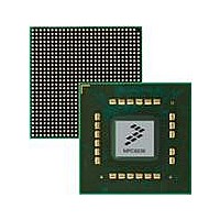
MPC8536DS Freescale Semiconductor, MPC8536DS Datasheet - Page 1629

MPC8536DS
Manufacturer Part Number
MPC8536DS
Description
BOARD DEV SYSTEM MPC8536E
Manufacturer
Freescale Semiconductor
Series
PowerQUICC III™r
Type
MPUr
Datasheets
1.MPC8536EBVTAVLA.pdf
(127 pages)
2.MPC8536EBVTAVLA.pdf
(1706 pages)
3.MPC8536DS.pdf
(2 pages)
4.MPC8536DS.pdf
(126 pages)
Specifications of MPC8536DS
Contents
Board, Software and Documentation
Processor Series
MPC85xx
Core
e500
Data Bus Width
32 bit
Maximum Clock Frequency
667 MHz
Operating Supply Voltage
- 0.3 V to + 1.21 V
Maximum Operating Temperature
+ 105 C
Data Ram Size
32 KB
Interface Type
SPI, USB
Program Memory Type
DDR2, DDR3, SDRAM
Core Size
32 Bit
Program Memory Size
544KB
Cpu Speed
1.5GHz
Digital Ic Case Style
BGA
No. Of Pins
783
Supply Voltage Range
0.95V To 1.05V
Rohs Compliant
Yes
For Use With/related Products
MPC8536
Lead Free Status / RoHS Status
Lead free / RoHS Compliant
- MPC8536EBVTAVLA PDF datasheet
- MPC8536EBVTAVLA PDF datasheet #2
- MPC8536DS PDF datasheet #3
- MPC8536DS PDF datasheet #4
- Current page: 1629 of 1706
- Download datasheet (15Mb)
A.1.13
Freescale Semiconductor
SATA2 has the same memory-mapped registers that are described for SATA1 from 0x1_8000 to 0x1_8FFF except the offsets
are from 0x1_9000 to 0x1_9FFF.
0x10C
Offset
0xE00
0xE04
0x000
0x010
0x014
0x018
0x020
0x024
0x028
0x030
0x034
0x038
0x040
0x044
0x048
0x100
0x104
0x108
0x40C–
Offset
0xFFF
L2CTL—L2 control register
L2CEWAR0—L2 cache external write address register 0
L2CEWAREA0—L2 cache external write address register extended
address 0
L2CEWCR0—L2 cache external write control register 0
L2CEWAR1—L2 cache external write address register 1
L2CEWAREA1—L2 cache external write address register extended
address 1
L2CEWCR1—L2 cache external write control register 1
L2CEWAR2—L2 cache external write address register 2
L2CEWAREA2—L2 cache external write address register extended
address 2
L2CEWCR2—L2 cache external write control register 2
L2CEWAR3—L2 cache external write address register 3
L2CEWAREA3—L2 cache external write address register extended
address 3
L2CEWCR3—L2 cache external write control register 3
L2SRBAR0—L2 memory-mapped SRAM base address register 0
L2SRBAREA0—L2 memory-mapped SRAM base address register
extended address 0
L2SRBAR1—L2 memory-mapped SRAM base address register 1
L2SRBAREA1—L2 memory-mapped SRAM base address register
extended address 1
L2ERRINJHI—L2 error injection mask high register
L2ERRINJLO—L2 error injection mask low register
L2 Cache/SRAM
Reserved
L2/SRAM Memory-Mapped Configuration Registers—Block Base Address: 0x2_0000
MPC8536E PowerQUICC III Integrated Processor Reference Manual, Rev. 1
SATA Controller 1—Block Base Address 0x1_8000
SATA Controller 2—Block Base Address 0x1_9000
Table A-13. L2/SRAM Memory-Mapped Registers
Table A-12. SATA Registers (continued)
SATA2—Block Base Address: 0x1_9000
Register
Register
Complete List of Configuration, Control, and Status Registers
Access
—
Access
R/W
R/W
R/W
R/W
R/W
R/W
R/W
R/W
R/W
R/W
R/W
R/W
R/W
R/W
R/W
R/W
R/W
R/W
R/W
0x2000_0000
0x0000_0000
0x0000_0000
0x0000_0000
0x0000_0000
0x0000_0000
0x0000_0000
0x0000_0000
0x0000_0000
0x0000_0000
0x0000_0000
0x0000_0000
0x0000_0000
0x0000_0000
0x0000_0000
0x0000_0000
0x0000_0000
0x0000_0000
0x0000_0000
Reset
Reset
—
Section/Page
Section/Page
6.3.1.2.1/6-13
6.3.1.2.2/6-14
6.3.1.2.3/6-14
6.3.1.2.1/6-13
6.3.1.2.2/6-14
6.3.1.2.3/6-14
6.3.1.2.1/6-13
6.3.1.2.2/6-14
6.3.1.2.3/6-14
6.3.1.2.1/6-13
6.3.1.2.2/6-14
6.3.1.2.3/6-14
6.3.1.3.1/6-16
6.3.1.3.2/6-17
6.3.1.3.1/6-16
6.3.1.3.2/6-17
6.3.1.4.1/6-18
6.3.1.4.1/6-18
6.3.1.1/6-10
—
A-17
Related parts for MPC8536DS
Image
Part Number
Description
Manufacturer
Datasheet
Request
R
Part Number:
Description:
Manufacturer:
Freescale Semiconductor, Inc
Datasheet:
Part Number:
Description:
Manufacturer:
Freescale Semiconductor, Inc
Datasheet:
Part Number:
Description:
Manufacturer:
Freescale Semiconductor, Inc
Datasheet:
Part Number:
Description:
Manufacturer:
Freescale Semiconductor, Inc
Datasheet:
Part Number:
Description:
Manufacturer:
Freescale Semiconductor, Inc
Datasheet:
Part Number:
Description:
Manufacturer:
Freescale Semiconductor, Inc
Datasheet:
Part Number:
Description:
Manufacturer:
Freescale Semiconductor, Inc
Datasheet:
Part Number:
Description:
Manufacturer:
Freescale Semiconductor, Inc
Datasheet:
Part Number:
Description:
Manufacturer:
Freescale Semiconductor, Inc
Datasheet:
Part Number:
Description:
Manufacturer:
Freescale Semiconductor, Inc
Datasheet:
Part Number:
Description:
Manufacturer:
Freescale Semiconductor, Inc
Datasheet:
Part Number:
Description:
Manufacturer:
Freescale Semiconductor, Inc
Datasheet:
Part Number:
Description:
Manufacturer:
Freescale Semiconductor, Inc
Datasheet:
Part Number:
Description:
Manufacturer:
Freescale Semiconductor, Inc
Datasheet:
Part Number:
Description:
Manufacturer:
Freescale Semiconductor, Inc
Datasheet:


