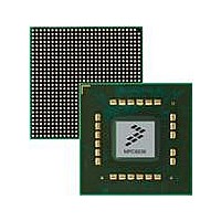
MPC8536DS Freescale Semiconductor, MPC8536DS Datasheet - Page 1649

MPC8536DS
Manufacturer Part Number
MPC8536DS
Description
BOARD DEV SYSTEM MPC8536E
Manufacturer
Freescale Semiconductor
Series
PowerQUICC III™r
Type
MPUr
Datasheets
1.MPC8536EBVTAVLA.pdf
(127 pages)
2.MPC8536EBVTAVLA.pdf
(1706 pages)
3.MPC8536DS.pdf
(2 pages)
4.MPC8536DS.pdf
(126 pages)
Specifications of MPC8536DS
Contents
Board, Software and Documentation
Processor Series
MPC85xx
Core
e500
Data Bus Width
32 bit
Maximum Clock Frequency
667 MHz
Operating Supply Voltage
- 0.3 V to + 1.21 V
Maximum Operating Temperature
+ 105 C
Data Ram Size
32 KB
Interface Type
SPI, USB
Program Memory Type
DDR2, DDR3, SDRAM
Core Size
32 Bit
Program Memory Size
544KB
Cpu Speed
1.5GHz
Digital Ic Case Style
BGA
No. Of Pins
783
Supply Voltage Range
0.95V To 1.05V
Rohs Compliant
Yes
For Use With/related Products
MPC8536
Lead Free Status / RoHS Status
Lead free / RoHS Compliant
- MPC8536EBVTAVLA PDF datasheet
- MPC8536EBVTAVLA PDF datasheet #2
- MPC8536DS PDF datasheet #3
- MPC8536DS PDF datasheet #4
- Current page: 1649 of 1706
- Download datasheet (15Mb)
A.2
The programmable interrupt controller (PIC) follows the OpenPIC programming model which requires a
larger register address space than the 4 Kbytes allocated to other blocks within the general utilities space.
For this reason, the PIC is allocated the second 256 Kbytes of CCSR space (0x4_0000–0x6_FFFF).
A.2.1
Freescale Semiconductor
0x0020–
1
2
0x0000
0x0010
0x0030
Byte Address Offset
0x3_F800–0x3_FFFF
Offset
Byte accessibility is controlled by internal logic, particularly at FIFOs, to prevent unintended overwrites of partial words
during writes, and to prevent unintended duplicate reads of partial data during reads. In addition, these bytes must be
presented on the correct byte lanes for the intended destination.
For the EU FIFOs, write operations anywhere in the address range enqueue to the input FIFO, and read operations
anywhere in the address range dequeue from the output FIFO. See the referenced section for more detailed
information.
(AD 17–0)
0x3_F000
0x3_F008
0x3_F010
0x3_F018
0x3_F020
0x3_F028
0x3_F030
0x3_F038
0x3_F040
0x3_F050
0x3_F108
0x3_F400
Programmable Interrupt Controller (PIC)
PIC—Global Registers
BRR1—Block revision register 1
BRR2—Block revision register 2
Reserved
MPC8536E PowerQUICC III Integrated Processor Reference Manual, Rev. 1
PIC Global Registers—Block Base Address 0x4_0000
Module
CRCU
Table 1-4. SEC Address Map (continued)
Register
Mode register
Key size register
Data size register
Reset control register
Control
Status register
Interrupt status register
Interrupt mask register
ICV size register
End of message register
Context register
Key register
Input FIFO
Table A-14. PIC Global Registers
Register
Complete List of Configuration, Control, and Status Registers
Access
Access
R/W
R/W
R/W
R/W
R/W
R/W
R/W
R/W
R/W
R/W
W
W
R
—
R
R
1
Write
word
word
word
word
word
word
word
word
word
byte
byte
byte
by
—
0x0040_0300
0x0000_0001
Reset
—
10.7.3.11/10-106
10.7.3.12/10-106
10.7.3.13/10-108
10.7.3.14/10-108
10.7.3.4/10-100
10.7.3.5/10-100
10.7.3.6/10-101
10.7.3.7/10-101
10.7.3.8/10-102
10.7.3.9/10-104
10.7.3.2/10-98
10.7.3.3/10-99
10.7.1.9/10-67
Reference
Section/Page
9.3.1.1/9-19
9.3.1.2/9-19
—
A-37
Related parts for MPC8536DS
Image
Part Number
Description
Manufacturer
Datasheet
Request
R
Part Number:
Description:
Manufacturer:
Freescale Semiconductor, Inc
Datasheet:
Part Number:
Description:
Manufacturer:
Freescale Semiconductor, Inc
Datasheet:
Part Number:
Description:
Manufacturer:
Freescale Semiconductor, Inc
Datasheet:
Part Number:
Description:
Manufacturer:
Freescale Semiconductor, Inc
Datasheet:
Part Number:
Description:
Manufacturer:
Freescale Semiconductor, Inc
Datasheet:
Part Number:
Description:
Manufacturer:
Freescale Semiconductor, Inc
Datasheet:
Part Number:
Description:
Manufacturer:
Freescale Semiconductor, Inc
Datasheet:
Part Number:
Description:
Manufacturer:
Freescale Semiconductor, Inc
Datasheet:
Part Number:
Description:
Manufacturer:
Freescale Semiconductor, Inc
Datasheet:
Part Number:
Description:
Manufacturer:
Freescale Semiconductor, Inc
Datasheet:
Part Number:
Description:
Manufacturer:
Freescale Semiconductor, Inc
Datasheet:
Part Number:
Description:
Manufacturer:
Freescale Semiconductor, Inc
Datasheet:
Part Number:
Description:
Manufacturer:
Freescale Semiconductor, Inc
Datasheet:
Part Number:
Description:
Manufacturer:
Freescale Semiconductor, Inc
Datasheet:
Part Number:
Description:
Manufacturer:
Freescale Semiconductor, Inc
Datasheet:


