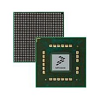
MPC8536DS Freescale Semiconductor, MPC8536DS Datasheet - Page 228

MPC8536DS
Manufacturer Part Number
MPC8536DS
Description
BOARD DEV SYSTEM MPC8536E
Manufacturer
Freescale Semiconductor
Series
PowerQUICC III™r
Type
MPUr
Datasheets
1.MPC8536EBVTAVLA.pdf
(127 pages)
2.MPC8536EBVTAVLA.pdf
(1706 pages)
3.MPC8536DS.pdf
(2 pages)
4.MPC8536DS.pdf
(126 pages)
Specifications of MPC8536DS
Contents
Board, Software and Documentation
Processor Series
MPC85xx
Core
e500
Data Bus Width
32 bit
Maximum Clock Frequency
667 MHz
Operating Supply Voltage
- 0.3 V to + 1.21 V
Maximum Operating Temperature
+ 105 C
Data Ram Size
32 KB
Interface Type
SPI, USB
Program Memory Type
DDR2, DDR3, SDRAM
Core Size
32 Bit
Program Memory Size
544KB
Cpu Speed
1.5GHz
Digital Ic Case Style
BGA
No. Of Pins
783
Supply Voltage Range
0.95V To 1.05V
Rohs Compliant
Yes
For Use With/related Products
MPC8536
Lead Free Status / RoHS Status
Lead free / RoHS Compliant
- MPC8536EBVTAVLA PDF datasheet
- MPC8536EBVTAVLA PDF datasheet #2
- MPC8536DS PDF datasheet #3
- MPC8536DS PDF datasheet #4
- Current page: 228 of 1706
- Download datasheet (15Mb)
L2 Look-Aside Cache/SRAM
The L2/SRAM can be accessed by the e500 core or the system interface through the ECM. The L2 cache
does not initiate transactions.
Figure 6-6
In SRAM mode, if a non–cache-line read or write transaction is not preceded by a cache-line write, an ECC
error occurs; such a non–cache-line write transaction cannot be allocated in the L2.
6.3
Table 6-3
In this table and in the register figures and field descriptions, the following access definitions apply:
6-8
.
•
•
•
•
•
Reserved fields are always ignored for the purposes of determining access type.
R/W, R, and W (read/write, read only, and write only) indicate that all the non-reserved fields in a
register have the same access type.
w1c indicates that all of the non-reserved fields in a register are cleared by writing ones to them.
Mixed indicates a combination of access types.
Special is used when no other category applies. In this case the register figure and field description
table should be read carefully.
shows the memory map for the L2/SRAM registers.
shows address connections of the e500 core and L2/SRAM.
Memory Map/Register Definition
MPC8536E PowerQUICC III Integrated Processor Reference Manual, Rev. 1
e500 Coherency Module
e500 Coherency Module
SNOOP
RD1
e500 Core
Figure 6-5
(ECM)
Figure 6-6. Address Bus Connection of CCB
e500 Core
(ECM)
Figure 6-5. Data Bus Connection of CCB
RD2
MSTR
WR
shows the data bus connections of the e500 core and L2/SRAM.
128
128
64
RD IN
L2/SRAM
DOUT WR IN
ADDR_IN
L2/SRAM
Freescale Semiconductor
Related parts for MPC8536DS
Image
Part Number
Description
Manufacturer
Datasheet
Request
R
Part Number:
Description:
Manufacturer:
Freescale Semiconductor, Inc
Datasheet:
Part Number:
Description:
Manufacturer:
Freescale Semiconductor, Inc
Datasheet:
Part Number:
Description:
Manufacturer:
Freescale Semiconductor, Inc
Datasheet:
Part Number:
Description:
Manufacturer:
Freescale Semiconductor, Inc
Datasheet:
Part Number:
Description:
Manufacturer:
Freescale Semiconductor, Inc
Datasheet:
Part Number:
Description:
Manufacturer:
Freescale Semiconductor, Inc
Datasheet:
Part Number:
Description:
Manufacturer:
Freescale Semiconductor, Inc
Datasheet:
Part Number:
Description:
Manufacturer:
Freescale Semiconductor, Inc
Datasheet:
Part Number:
Description:
Manufacturer:
Freescale Semiconductor, Inc
Datasheet:
Part Number:
Description:
Manufacturer:
Freescale Semiconductor, Inc
Datasheet:
Part Number:
Description:
Manufacturer:
Freescale Semiconductor, Inc
Datasheet:
Part Number:
Description:
Manufacturer:
Freescale Semiconductor, Inc
Datasheet:
Part Number:
Description:
Manufacturer:
Freescale Semiconductor, Inc
Datasheet:
Part Number:
Description:
Manufacturer:
Freescale Semiconductor, Inc
Datasheet:
Part Number:
Description:
Manufacturer:
Freescale Semiconductor, Inc
Datasheet:


