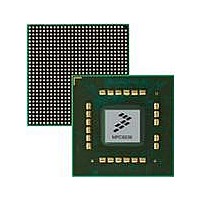
MPC8536DS Freescale Semiconductor, MPC8536DS Datasheet - Page 217

MPC8536DS
Manufacturer Part Number
MPC8536DS
Description
BOARD DEV SYSTEM MPC8536E
Manufacturer
Freescale Semiconductor
Series
PowerQUICC III™r
Type
MPUr
Datasheets
1.MPC8536EBVTAVLA.pdf
(127 pages)
2.MPC8536EBVTAVLA.pdf
(1706 pages)
3.MPC8536DS.pdf
(2 pages)
4.MPC8536DS.pdf
(126 pages)
Specifications of MPC8536DS
Contents
Board, Software and Documentation
Processor Series
MPC85xx
Core
e500
Data Bus Width
32 bit
Maximum Clock Frequency
667 MHz
Operating Supply Voltage
- 0.3 V to + 1.21 V
Maximum Operating Temperature
+ 105 C
Data Ram Size
32 KB
Interface Type
SPI, USB
Program Memory Type
DDR2, DDR3, SDRAM
Core Size
32 Bit
Program Memory Size
544KB
Cpu Speed
1.5GHz
Digital Ic Case Style
BGA
No. Of Pins
783
Supply Voltage Range
0.95V To 1.05V
Rohs Compliant
Yes
For Use With/related Products
MPC8536
Lead Free Status / RoHS Status
Lead free / RoHS Compliant
- MPC8536EBVTAVLA PDF datasheet
- MPC8536EBVTAVLA PDF datasheet #2
- MPC8536DS PDF datasheet #3
- MPC8536DS PDF datasheet #4
- Current page: 217 of 1706
- Download datasheet (15Mb)
5.2
The CCB is the hardware interface between the core and the SoC, and with a few exceptions, the user
cannot access these internal signals directly.
in various places in this manual and in the e500 Reference Manual because understanding how they work
helps the reader understand the functionality of the device. Links to other chapters in this manual are
provided in
Aspects of the e500–SoC integration are summarized in the following:
Freescale Semiconductor
•
•
•
Reset. The core directs and coordinates device hard and soft resets and the power-on reset (POR)
sequence, power-on reset configuration, and initialization. Core integration of the reset signals
shown in
Chapter 23, “Global
Clocking and timers. Integration details of the CCB clocking signals are described in
“Reset, Clocking, and
in
Cache and memory-mapped SRAM. The e500 cache implementation interacts with the SoC’s L2
cache. In particular, the core implements a number of instructions that interact with the L2 cache
implementation, which are described in the e500 Reference Manual and in the EREF.
“L2 Look-Aside Cache/SRAM,”
that interface with the L2 cache.
Section 5.3, “Summary of Core Integratation
e500 Core Integration and the Core Complex Bus (CCB)
Figure 5-2
Chapter 25, “Debug
Chapter 25, “Debug
Watchpoint Facility”
Watchpoint Facility”
Figure 5-2
JTAG and TAP
Test and Debug
Features and
Features and
MPC8536E PowerQUICC III Integrated Processor Reference Manual, Rev. 1
Address Bus
and in the text that follows.
Master
are described
Utilities.”
Initialization.” Addition details regarding timer configuration are described
Figure 5-2. e500 Core Integration
describes the SoC’s L2 cache.
tt [0:4]
gbl
ci
ts
wt
cl
Chapter 4, “Reset, Clocking, and
trst
tck
tms
tdi
tdo
tdo_ien
tlmsel
tap_en
waitr
ude
ckstp_out
clkout
Selected CCB Signals
Figure 5-2
core_fault_in
pll_cfg [0:5]
hreset_req
pm_event
pvr [0:31]
shows a selection of CCB signals that are discussed
svr [0:31]
stopped
wrs [0:1]
Details.”
pll_clk
hreset
halted
sleep
doze
tbclk
tben
tbint
mcp
stop
nap
halt
cint
int
Figure 5-2
Clocking
Chapter 4, “Reset, Clocking,
and
Time base/watchdog timer
Chapter 4, “Reset, Clocking,
and Initialization”
External Interrupts
Chapter 9, “Programmable
Interrupt Controller
Power management
Chapter 23, “Global
Miscellaneous
Chapter 23, “Global
Initialization,” and in
Initialization”
shows the e500 signals
e500 Core Integration Details
(PIC)”
Utilities”
Utilities”
Chapter 4,
Chapter 6,
5-3
Related parts for MPC8536DS
Image
Part Number
Description
Manufacturer
Datasheet
Request
R
Part Number:
Description:
Manufacturer:
Freescale Semiconductor, Inc
Datasheet:
Part Number:
Description:
Manufacturer:
Freescale Semiconductor, Inc
Datasheet:
Part Number:
Description:
Manufacturer:
Freescale Semiconductor, Inc
Datasheet:
Part Number:
Description:
Manufacturer:
Freescale Semiconductor, Inc
Datasheet:
Part Number:
Description:
Manufacturer:
Freescale Semiconductor, Inc
Datasheet:
Part Number:
Description:
Manufacturer:
Freescale Semiconductor, Inc
Datasheet:
Part Number:
Description:
Manufacturer:
Freescale Semiconductor, Inc
Datasheet:
Part Number:
Description:
Manufacturer:
Freescale Semiconductor, Inc
Datasheet:
Part Number:
Description:
Manufacturer:
Freescale Semiconductor, Inc
Datasheet:
Part Number:
Description:
Manufacturer:
Freescale Semiconductor, Inc
Datasheet:
Part Number:
Description:
Manufacturer:
Freescale Semiconductor, Inc
Datasheet:
Part Number:
Description:
Manufacturer:
Freescale Semiconductor, Inc
Datasheet:
Part Number:
Description:
Manufacturer:
Freescale Semiconductor, Inc
Datasheet:
Part Number:
Description:
Manufacturer:
Freescale Semiconductor, Inc
Datasheet:
Part Number:
Description:
Manufacturer:
Freescale Semiconductor, Inc
Datasheet:


