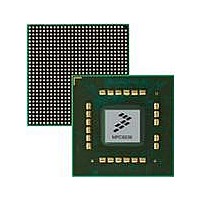
MPC8536DS Freescale Semiconductor, MPC8536DS Datasheet - Page 281

MPC8536DS
Manufacturer Part Number
MPC8536DS
Description
BOARD DEV SYSTEM MPC8536E
Manufacturer
Freescale Semiconductor
Series
PowerQUICC III™r
Type
MPUr
Datasheets
1.MPC8536EBVTAVLA.pdf
(127 pages)
2.MPC8536EBVTAVLA.pdf
(1706 pages)
3.MPC8536DS.pdf
(2 pages)
4.MPC8536DS.pdf
(126 pages)
Specifications of MPC8536DS
Contents
Board, Software and Documentation
Processor Series
MPC85xx
Core
e500
Data Bus Width
32 bit
Maximum Clock Frequency
667 MHz
Operating Supply Voltage
- 0.3 V to + 1.21 V
Maximum Operating Temperature
+ 105 C
Data Ram Size
32 KB
Interface Type
SPI, USB
Program Memory Type
DDR2, DDR3, SDRAM
Core Size
32 Bit
Program Memory Size
544KB
Cpu Speed
1.5GHz
Digital Ic Case Style
BGA
No. Of Pins
783
Supply Voltage Range
0.95V To 1.05V
Rohs Compliant
Yes
For Use With/related Products
MPC8536
Lead Free Status / RoHS Status
Lead free / RoHS Compliant
- MPC8536EBVTAVLA PDF datasheet
- MPC8536EBVTAVLA PDF datasheet #2
- MPC8536DS PDF datasheet #3
- MPC8536DS PDF datasheet #4
- Current page: 281 of 1706
- Download datasheet (15Mb)
Freescale Semiconductor
MECC[0:7]
MBA[2:0]
MA[15:0]
Signal
Table 8-3. Memory Interface Signals—Detailed Signal Descriptions (continued)
I/O
I/O Error checking and correcting codes. Input and output signals for the DDR controller’s bidirectional ECC
O
O
O
I
MPC8536E PowerQUICC III Integrated Processor Reference Manual, Rev. 1
bus. MECC[0:5] function in both normal and debug modes.
As normal mode outputs the ECC signals represent the state of ECC driven by the DDR controller on
writes. As debug mode outputs MECC[0:5] provide source ID and data-valid information. See
Section 8.5.11, “Error Checking and Correcting
ECC Pins,”
As inputs, the ECC signals represent the state of ECC driven by the SDRAM devices on reads.
Address bus. Memory controller outputs for the address to the DRAM. MA[15:0] carry 16 of the address
bits for the DDR memory interface corresponding to the row and column address bits. MA0 is the lsb of
the address output from the memory controller.
Logical bank address. Outputs that drive the logical (or internal) bank address pins of the SDRAM. Each
SDRAM supports four or eight addressable logical sub-banks. Bit zero of the memory controller’s output
bank address must be connected to bit zero of the SDRAM’s input bank address. MBA0, the
least-significant bit of the three bank address signals, is asserted during the mode register set command
to specify the extended mode register.
Meaning
Meaning
Meaning
Meaning
Timing Assertion/Negation—Same timing as MDQ
Timing Assertion/Negation—Same timing as MDQ
Timing Assertion/Negation—The address lines are only driven when the controller has a command
Timing Assertion/Negation—Same timing as MA n
State
State
State
State
Asserted/Negated—Represents the state of ECC being driven by the DDR controller on
High impedance—Same timing as MDQ
Asserted/Negated—Represents the state of ECC being driven by the DDR SDRAMs on
High impedance—Same timing as MDQ
Asserted/Negated—Represents the address driven by the DDR memory controller. Contains
High impedance—When the memory controller is disabled
Asserted/Negated—Selects the DDR SDRAM logical (or internal) bank to be activated during
High impedance—Same timing as MA n
for more details.
writes.
reads.
different portions of the address depending on the memory size and the DRAM
command being issued by the memory controller. See
description of the mapping of these signals.
scheduled to issue on the address/CMD bus; otherwise they will be at high-Z. It is valid
when a transaction is driven to DRAM (when MCS n is active).
the row address phase and selects the SDRAM internal bank for the read or write
operation during the column address phase of the memory access.
describes the mapping of these signals in all cases.
Description
(ECC),” and
Section 25.4.2.2, “Debug Information on
Table 8-55
DDR Memory Controller
for a complete
Table 8-55
8-7
Related parts for MPC8536DS
Image
Part Number
Description
Manufacturer
Datasheet
Request
R
Part Number:
Description:
Manufacturer:
Freescale Semiconductor, Inc
Datasheet:
Part Number:
Description:
Manufacturer:
Freescale Semiconductor, Inc
Datasheet:
Part Number:
Description:
Manufacturer:
Freescale Semiconductor, Inc
Datasheet:
Part Number:
Description:
Manufacturer:
Freescale Semiconductor, Inc
Datasheet:
Part Number:
Description:
Manufacturer:
Freescale Semiconductor, Inc
Datasheet:
Part Number:
Description:
Manufacturer:
Freescale Semiconductor, Inc
Datasheet:
Part Number:
Description:
Manufacturer:
Freescale Semiconductor, Inc
Datasheet:
Part Number:
Description:
Manufacturer:
Freescale Semiconductor, Inc
Datasheet:
Part Number:
Description:
Manufacturer:
Freescale Semiconductor, Inc
Datasheet:
Part Number:
Description:
Manufacturer:
Freescale Semiconductor, Inc
Datasheet:
Part Number:
Description:
Manufacturer:
Freescale Semiconductor, Inc
Datasheet:
Part Number:
Description:
Manufacturer:
Freescale Semiconductor, Inc
Datasheet:
Part Number:
Description:
Manufacturer:
Freescale Semiconductor, Inc
Datasheet:
Part Number:
Description:
Manufacturer:
Freescale Semiconductor, Inc
Datasheet:
Part Number:
Description:
Manufacturer:
Freescale Semiconductor, Inc
Datasheet:


