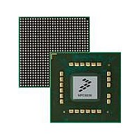
MPC8536DS Freescale Semiconductor, MPC8536DS Datasheet - Page 738

MPC8536DS
Manufacturer Part Number
MPC8536DS
Description
BOARD DEV SYSTEM MPC8536E
Manufacturer
Freescale Semiconductor
Series
PowerQUICC III™r
Type
MPUr
Datasheets
1.MPC8536EBVTAVLA.pdf
(127 pages)
2.MPC8536EBVTAVLA.pdf
(1706 pages)
3.MPC8536DS.pdf
(2 pages)
4.MPC8536DS.pdf
(126 pages)
Specifications of MPC8536DS
Contents
Board, Software and Documentation
Processor Series
MPC85xx
Core
e500
Data Bus Width
32 bit
Maximum Clock Frequency
667 MHz
Operating Supply Voltage
- 0.3 V to + 1.21 V
Maximum Operating Temperature
+ 105 C
Data Ram Size
32 KB
Interface Type
SPI, USB
Program Memory Type
DDR2, DDR3, SDRAM
Core Size
32 Bit
Program Memory Size
544KB
Cpu Speed
1.5GHz
Digital Ic Case Style
BGA
No. Of Pins
783
Supply Voltage Range
0.95V To 1.05V
Rohs Compliant
Yes
For Use With/related Products
MPC8536
Lead Free Status / RoHS Status
Lead free / RoHS Compliant
- MPC8536EBVTAVLA PDF datasheet
- MPC8536EBVTAVLA PDF datasheet #2
- MPC8536DS PDF datasheet #3
- MPC8536DS PDF datasheet #4
- Current page: 738 of 1706
- Download datasheet (15Mb)
Enhanced Local Bus Controller
13.5.4.2
An example of configuring FCM to execute a status read command to large-page NAND Flash is shown
in
Flash status into register MDR[AS0]. The sequence is initiated by writing FMR[OP] = 10 and issuing a
special operation to the bank. At the conclusion of the sequence, eLBC will issue a command complete
interrupt (LTESR[CC]) if interrupts are enabled.
13.5.4.3
An example of configuring FCM to execute a status ID command to large-page NAND Flash is shown in
Table
a dummy address prior to the sequence, and then to receive the first 4 bytes of ID during the sequence. The
sequence is initiated by writing FMR[OP] = 10, and issuing a special operation to the bank. At the
conclusion of the sequence, eLBC will issue a command complete interrupt (LTESR[CC]) if interrupts are
enabled. MDR[AS3–AS0] then can be read to obtain the first 4 bytes of NAND Flash ID.
13-96
Table
13-46. This sequence does not require use of the shared FCM buffer RAM, but uses MDR to set up
13-45. This sequence does not require use of the shared FCM buffer RAM, but reads the NAND
Register
Register
Register
FBCR
FBCR
FBAR
FBAR
FPAR
FPAR
FPAR
MDR
MDR
NAND Flash Read Status Command Sequence Example
FCR
NAND Flash Read Identification Command Sequence Example
FCR
FIR
FIR
Table 13-44. FCM Register Settings for Soft Reset (OR n [PGS] = 1) (continued)
Table 13-45. FCM Register Settings for Status Read (OR n [PGS] = 1)
MPC8536E PowerQUICC III Integrated Processor Reference Manual, Rev. 1
Table 13-46. FCM Register Settings for ID Read (OR n [PGS] = 1)
Initial Contents
Initial Contents
Initial Contents
0x40000000
0x70000000
0x4B000000
0x90000000
—
—
—
—
—
—
—
—
—
unused
unused
unused
OP0 = CM0 = command 0;
OP1–OP7 = NOP
CMD0 = 0x70 = read status command; other commands unused
unused
unused
unused
Status returned in AS0
OP0 = CM0 = command 0;
OP1 = RS = read status to MDR;
OP2–OP7 = NOP
CMD0 = 0x90 = read ID command; other commands unused
unused
unused
Description
Description
Description
Freescale Semiconductor
Related parts for MPC8536DS
Image
Part Number
Description
Manufacturer
Datasheet
Request
R
Part Number:
Description:
Manufacturer:
Freescale Semiconductor, Inc
Datasheet:
Part Number:
Description:
Manufacturer:
Freescale Semiconductor, Inc
Datasheet:
Part Number:
Description:
Manufacturer:
Freescale Semiconductor, Inc
Datasheet:
Part Number:
Description:
Manufacturer:
Freescale Semiconductor, Inc
Datasheet:
Part Number:
Description:
Manufacturer:
Freescale Semiconductor, Inc
Datasheet:
Part Number:
Description:
Manufacturer:
Freescale Semiconductor, Inc
Datasheet:
Part Number:
Description:
Manufacturer:
Freescale Semiconductor, Inc
Datasheet:
Part Number:
Description:
Manufacturer:
Freescale Semiconductor, Inc
Datasheet:
Part Number:
Description:
Manufacturer:
Freescale Semiconductor, Inc
Datasheet:
Part Number:
Description:
Manufacturer:
Freescale Semiconductor, Inc
Datasheet:
Part Number:
Description:
Manufacturer:
Freescale Semiconductor, Inc
Datasheet:
Part Number:
Description:
Manufacturer:
Freescale Semiconductor, Inc
Datasheet:
Part Number:
Description:
Manufacturer:
Freescale Semiconductor, Inc
Datasheet:
Part Number:
Description:
Manufacturer:
Freescale Semiconductor, Inc
Datasheet:
Part Number:
Description:
Manufacturer:
Freescale Semiconductor, Inc
Datasheet:


