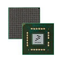
MPC8536DS Freescale Semiconductor, MPC8536DS Datasheet - Page 320

MPC8536DS
Manufacturer Part Number
MPC8536DS
Description
BOARD DEV SYSTEM MPC8536E
Manufacturer
Freescale Semiconductor
Series
PowerQUICC III™r
Type
MPUr
Datasheets
1.MPC8536EBVTAVLA.pdf
(127 pages)
2.MPC8536EBVTAVLA.pdf
(1706 pages)
3.MPC8536DS.pdf
(2 pages)
4.MPC8536DS.pdf
(126 pages)
Specifications of MPC8536DS
Contents
Board, Software and Documentation
Processor Series
MPC85xx
Core
e500
Data Bus Width
32 bit
Maximum Clock Frequency
667 MHz
Operating Supply Voltage
- 0.3 V to + 1.21 V
Maximum Operating Temperature
+ 105 C
Data Ram Size
32 KB
Interface Type
SPI, USB
Program Memory Type
DDR2, DDR3, SDRAM
Core Size
32 Bit
Program Memory Size
544KB
Cpu Speed
1.5GHz
Digital Ic Case Style
BGA
No. Of Pins
783
Supply Voltage Range
0.95V To 1.05V
Rohs Compliant
Yes
For Use With/related Products
MPC8536
Lead Free Status / RoHS Status
Lead free / RoHS Compliant
- MPC8536EBVTAVLA PDF datasheet
- MPC8536EBVTAVLA PDF datasheet #2
- MPC8536DS PDF datasheet #3
- MPC8536DS PDF datasheet #4
- Current page: 320 of 1706
- Download datasheet (15Mb)
DDR Memory Controller
8.4.1.25
The DDRDSR_1 register, shown in
the current settings of the P and N FET impedance for MDICn, command/control, and data.
Table 8-31
8-46
Offset 0xB20
Reset
12–15
16–19
20–23
24–27
28–31
Bits
W
R DDRDC
0
describes the DDRDSR_1 fields.
1
RCW11
RCW12
RCW13
RCW14
RCW15
10–15
16–19
20–23
24–27
28–31
Name
DDR Debug Status Register 1 (DDRDSR_1)
Bits
0–1
2–5
6–9
2
Table 8-30. DDR_Register Control Word 2 Field Descriptions (continued)
MDICPZ
MPC8536E PowerQUICC III Integrated Processor Reference Manual, Rev. 1
Register Control Word 0. Represents the value that is placed on MBA[1], MBA[0], MA[4], and
MA[3] during writes to register control word 11.
Register Control Word 0. Represents the value that is placed on MBA[1], MBA[0], MA[4], and
MA[3] during writes to register control word 12.
Register Control Word 0. Represents the value that is placed on MBA[1], MBA[0], MA[4], and
MA[3] during writes to register control word 13.
Register Control Word 0. Represents the value that is placed on MBA[1], MBA[0], MA[4], and
MA[3] during writes to register control word 14.
Register Control Word 0. Represents the value that is placed on MBA[1], MBA[0], MA[4], and
MA[3] during writes to register control word 15.
5
MDICPZ
MDICNZ
DDRDC
Figure 8-26. DDR Debug Status Register 1 (DDRDSR_1)
Name
CPZ
CNZ
DPZ
DNZ
—
6
MDICNZ
Table 8-31. DDRDSR_1 Field Descriptions
DDR driver compensation input value
Current setting of PFET driver MDIC impedance
Current setting of NFET driver MDIC impedance
Reserved, should be cleared.
Current setting of PFET driver command impedance
Current setting of NFET driver command impedance
Current setting of PFET driver data impedance
Current setting of NFET driver data impedance
Figure
9
10
8-26, contains the DDR driver compensation input value and
—
All zeros
15 16
Description
Description
CPZ
19 20
CNZ
23 24
Freescale Semiconductor
DPZ
Access: Read only
27 28
DNZ
31
Related parts for MPC8536DS
Image
Part Number
Description
Manufacturer
Datasheet
Request
R
Part Number:
Description:
Manufacturer:
Freescale Semiconductor, Inc
Datasheet:
Part Number:
Description:
Manufacturer:
Freescale Semiconductor, Inc
Datasheet:
Part Number:
Description:
Manufacturer:
Freescale Semiconductor, Inc
Datasheet:
Part Number:
Description:
Manufacturer:
Freescale Semiconductor, Inc
Datasheet:
Part Number:
Description:
Manufacturer:
Freescale Semiconductor, Inc
Datasheet:
Part Number:
Description:
Manufacturer:
Freescale Semiconductor, Inc
Datasheet:
Part Number:
Description:
Manufacturer:
Freescale Semiconductor, Inc
Datasheet:
Part Number:
Description:
Manufacturer:
Freescale Semiconductor, Inc
Datasheet:
Part Number:
Description:
Manufacturer:
Freescale Semiconductor, Inc
Datasheet:
Part Number:
Description:
Manufacturer:
Freescale Semiconductor, Inc
Datasheet:
Part Number:
Description:
Manufacturer:
Freescale Semiconductor, Inc
Datasheet:
Part Number:
Description:
Manufacturer:
Freescale Semiconductor, Inc
Datasheet:
Part Number:
Description:
Manufacturer:
Freescale Semiconductor, Inc
Datasheet:
Part Number:
Description:
Manufacturer:
Freescale Semiconductor, Inc
Datasheet:
Part Number:
Description:
Manufacturer:
Freescale Semiconductor, Inc
Datasheet:


