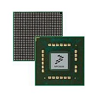
MPC8536DS Freescale Semiconductor, MPC8536DS Datasheet - Page 712

MPC8536DS
Manufacturer Part Number
MPC8536DS
Description
BOARD DEV SYSTEM MPC8536E
Manufacturer
Freescale Semiconductor
Series
PowerQUICC III™r
Type
MPUr
Datasheets
1.MPC8536EBVTAVLA.pdf
(127 pages)
2.MPC8536EBVTAVLA.pdf
(1706 pages)
3.MPC8536DS.pdf
(2 pages)
4.MPC8536DS.pdf
(126 pages)
Specifications of MPC8536DS
Contents
Board, Software and Documentation
Processor Series
MPC85xx
Core
e500
Data Bus Width
32 bit
Maximum Clock Frequency
667 MHz
Operating Supply Voltage
- 0.3 V to + 1.21 V
Maximum Operating Temperature
+ 105 C
Data Ram Size
32 KB
Interface Type
SPI, USB
Program Memory Type
DDR2, DDR3, SDRAM
Core Size
32 Bit
Program Memory Size
544KB
Cpu Speed
1.5GHz
Digital Ic Case Style
BGA
No. Of Pins
783
Supply Voltage Range
0.95V To 1.05V
Rohs Compliant
Yes
For Use With/related Products
MPC8536
Lead Free Status / RoHS Status
Lead free / RoHS Compliant
- MPC8536EBVTAVLA PDF datasheet
- MPC8536EBVTAVLA PDF datasheet #2
- MPC8536DS PDF datasheet #3
- MPC8536DS PDF datasheet #4
- Current page: 712 of 1706
- Download datasheet (15Mb)
Enhanced Local Bus Controller
13.4.3.3.3
Instructions CW0, CW1, RBW, and RSW force FCM to observe the state of the LFRB pin, which may be
driven low by a long-latency NAND Flash operation, such as a page read. Following the issue of such
commands, FCM waits as shown in
observing LFRB before it has been properly driven low by the device, but does not preclude LFRB from
remaining high after a command. In addition, FCM samples and compares the state of LFRB on two
consecutive cycles of LCLK to filter out noise on this signal as it rises to the ready state (LFRB = 1).
13.4.3.3.4
The timing for read data transfers is shown in
enable its output drivers and drive valid read data while LFRE is held low. FCM samples read data on the
rising edge of LFRE, which follows an optional number of wait states. Note that FCM will delay the first
read if a RBW or RSW instruction is issued, in which case LFRB sample timing takes effect (see
Section 13.4.3.3.3, “FCM Ready/Busy
13-70
LCLK
(unused)
LFCLE
LFALE
LFWE
LAD[0:7]
TA
LFCLE
LFWE
LFRB
LFRE
Figure 13-56. Example of FCM Command and Address Timing with Relaxed Parameters
FCM Ready/Busy Timing
FCM Read Data Timing
long-latency CW command issue
MPC8536E PowerQUICC III Integrated Processor Reference Manual, Rev. 1
TRLX = 0:
TRLX = 1:
Figure 13-57. FCM Delay Prior to Sampling LFRB State
8×(2+SCY) cycles
16×(2+SCY) LCLK cycles
(for TRLX = 1, CHT = 0, CST = 1, SCY = 2)
2×SCY = 4 cycles
Figure 13-57
Timing”).
command
Figure
LFRB sample
points
before sampling the state of LFRB. This guards against
13-58. Upon assertion of LFRE, the Flash device will
NAND FlashFlash busy state
ready state
FCM continues
following LFRB high
Freescale Semiconductor
address
Related parts for MPC8536DS
Image
Part Number
Description
Manufacturer
Datasheet
Request
R
Part Number:
Description:
Manufacturer:
Freescale Semiconductor, Inc
Datasheet:
Part Number:
Description:
Manufacturer:
Freescale Semiconductor, Inc
Datasheet:
Part Number:
Description:
Manufacturer:
Freescale Semiconductor, Inc
Datasheet:
Part Number:
Description:
Manufacturer:
Freescale Semiconductor, Inc
Datasheet:
Part Number:
Description:
Manufacturer:
Freescale Semiconductor, Inc
Datasheet:
Part Number:
Description:
Manufacturer:
Freescale Semiconductor, Inc
Datasheet:
Part Number:
Description:
Manufacturer:
Freescale Semiconductor, Inc
Datasheet:
Part Number:
Description:
Manufacturer:
Freescale Semiconductor, Inc
Datasheet:
Part Number:
Description:
Manufacturer:
Freescale Semiconductor, Inc
Datasheet:
Part Number:
Description:
Manufacturer:
Freescale Semiconductor, Inc
Datasheet:
Part Number:
Description:
Manufacturer:
Freescale Semiconductor, Inc
Datasheet:
Part Number:
Description:
Manufacturer:
Freescale Semiconductor, Inc
Datasheet:
Part Number:
Description:
Manufacturer:
Freescale Semiconductor, Inc
Datasheet:
Part Number:
Description:
Manufacturer:
Freescale Semiconductor, Inc
Datasheet:
Part Number:
Description:
Manufacturer:
Freescale Semiconductor, Inc
Datasheet:


