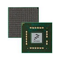
MPC8536DS Freescale Semiconductor, MPC8536DS Datasheet - Page 1526

MPC8536DS
Manufacturer Part Number
MPC8536DS
Description
BOARD DEV SYSTEM MPC8536E
Manufacturer
Freescale Semiconductor
Series
PowerQUICC III™r
Type
MPUr
Datasheets
1.MPC8536EBVTAVLA.pdf
(127 pages)
2.MPC8536EBVTAVLA.pdf
(1706 pages)
3.MPC8536DS.pdf
(2 pages)
4.MPC8536DS.pdf
(126 pages)
Specifications of MPC8536DS
Contents
Board, Software and Documentation
Processor Series
MPC85xx
Core
e500
Data Bus Width
32 bit
Maximum Clock Frequency
667 MHz
Operating Supply Voltage
- 0.3 V to + 1.21 V
Maximum Operating Temperature
+ 105 C
Data Ram Size
32 KB
Interface Type
SPI, USB
Program Memory Type
DDR2, DDR3, SDRAM
Core Size
32 Bit
Program Memory Size
544KB
Cpu Speed
1.5GHz
Digital Ic Case Style
BGA
No. Of Pins
783
Supply Voltage Range
0.95V To 1.05V
Rohs Compliant
Yes
For Use With/related Products
MPC8536
Lead Free Status / RoHS Status
Lead free / RoHS Compliant
- MPC8536EBVTAVLA PDF datasheet
- MPC8536EBVTAVLA PDF datasheet #2
- MPC8536DS PDF datasheet #3
- MPC8536DS PDF datasheet #4
- Current page: 1526 of 1706
- Download datasheet (15Mb)
Global Utilities
Table 23-29
23.4.1.27 General Control Register (GCR)
Shown in
Table 23-30
23-34
Offset 0xE60
Reset 0 0 0 0 0 0 0 0 0 0
10–11
Bits
0–9
12–15
16–19
20–23
24–31
8–11
Bits
0–3
4–7
W
R
0
Figure
ESDHC_UPRADR The uppermost bits of the ESDHC address bus for all transactions initiated by the ESDHC
describes the bit settings of ECMCR.
describes the bit settings of GCR.
SATA1_UPRADR
SATA2_UPRADR
USB1_UPRADR
USB2_UPRADR
USB3_UPRADR
BYPASS
Name
—
23-27, GCR contains control bits used for pad control of deep sleep power-saving mode.
Name
—
—
MPC8536E PowerQUICC III Integrated Processor Reference Manual, Rev. 1
Reserved
Bypass mode
Transactions eligible for bypassing other transactions are defined as follows:
00 Disable all bypassing (default).
01 Small read requests can bypass large requests from other on-chip network (OCN) ports.
10 Small read requests and write-with-response requests can bypass large requests from
11 All small requests can bypass large requests from other on-chip network (OCN) ports.
Rules for transaction bypassing:
• Maintain ordering for a given port—A transaction cannot bypass another from the same
• Identify potential “control requests”—Transactions must be 32 bytes of less to bypass
• Guarantee forward progress—Once the subsequent entry in front of larger transaction in
The uppermost bits of the USB1 address bus for all transactions initiated by the USB1
The uppermost bits of the USB2 address bus for all transactions initiated by the USB2
The uppermost bits of the USB3 address bus for all transactions initiated by the USB3
The uppermost bits of the SATA1 address bus for all transactions initiated by the SATA1
The uppermost bits of the SATA2 address bus for all transactions initiated by the SATA2
Reserved
port.
another transaction.
the queue has been replaced by a bypassing transaction, the “do not pass” bit of the queue
entry of the larger transaction can no longer be bypassed. If the “do not pass” bit has been
set for the immediate next entry in the queue following a small request (32 bytes or less),
the “do not pass” bit of the small request is automatically set.
Figure 23-27. General Control Register (GCR)
9
other on-chip network (OCN) ports.
Table 23-29. ECMCR Field Descriptions
BYPASS
10
0
Table 23-30. GCR Field Descriptions
11
0
12
0 0 0 0 1 0 0 0 0
—
Description
Description
20
DEEPSLEEP_Z
21
0
22
0 0 0 0 0 0 0 0 0 0
Freescale Semiconductor
Access: Read/Write
—
31
Related parts for MPC8536DS
Image
Part Number
Description
Manufacturer
Datasheet
Request
R
Part Number:
Description:
Manufacturer:
Freescale Semiconductor, Inc
Datasheet:
Part Number:
Description:
Manufacturer:
Freescale Semiconductor, Inc
Datasheet:
Part Number:
Description:
Manufacturer:
Freescale Semiconductor, Inc
Datasheet:
Part Number:
Description:
Manufacturer:
Freescale Semiconductor, Inc
Datasheet:
Part Number:
Description:
Manufacturer:
Freescale Semiconductor, Inc
Datasheet:
Part Number:
Description:
Manufacturer:
Freescale Semiconductor, Inc
Datasheet:
Part Number:
Description:
Manufacturer:
Freescale Semiconductor, Inc
Datasheet:
Part Number:
Description:
Manufacturer:
Freescale Semiconductor, Inc
Datasheet:
Part Number:
Description:
Manufacturer:
Freescale Semiconductor, Inc
Datasheet:
Part Number:
Description:
Manufacturer:
Freescale Semiconductor, Inc
Datasheet:
Part Number:
Description:
Manufacturer:
Freescale Semiconductor, Inc
Datasheet:
Part Number:
Description:
Manufacturer:
Freescale Semiconductor, Inc
Datasheet:
Part Number:
Description:
Manufacturer:
Freescale Semiconductor, Inc
Datasheet:
Part Number:
Description:
Manufacturer:
Freescale Semiconductor, Inc
Datasheet:
Part Number:
Description:
Manufacturer:
Freescale Semiconductor, Inc
Datasheet:


