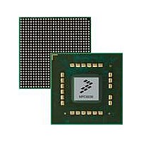
MPC8536DS Freescale Semiconductor, MPC8536DS Datasheet - Page 1631

MPC8536DS
Manufacturer Part Number
MPC8536DS
Description
BOARD DEV SYSTEM MPC8536E
Manufacturer
Freescale Semiconductor
Series
PowerQUICC III™r
Type
MPUr
Datasheets
1.MPC8536EBVTAVLA.pdf
(127 pages)
2.MPC8536EBVTAVLA.pdf
(1706 pages)
3.MPC8536DS.pdf
(2 pages)
4.MPC8536DS.pdf
(126 pages)
Specifications of MPC8536DS
Contents
Board, Software and Documentation
Processor Series
MPC85xx
Core
e500
Data Bus Width
32 bit
Maximum Clock Frequency
667 MHz
Operating Supply Voltage
- 0.3 V to + 1.21 V
Maximum Operating Temperature
+ 105 C
Data Ram Size
32 KB
Interface Type
SPI, USB
Program Memory Type
DDR2, DDR3, SDRAM
Core Size
32 Bit
Program Memory Size
544KB
Cpu Speed
1.5GHz
Digital Ic Case Style
BGA
No. Of Pins
783
Supply Voltage Range
0.95V To 1.05V
Rohs Compliant
Yes
For Use With/related Products
MPC8536
Lead Free Status / RoHS Status
Lead free / RoHS Compliant
- MPC8536EBVTAVLA PDF datasheet
- MPC8536EBVTAVLA PDF datasheet #2
- MPC8536DS PDF datasheet #3
- MPC8536DS PDF datasheet #4
- Current page: 1631 of 1706
- Download datasheet (15Mb)
Freescale Semiconductor
0x504–0xFFF
0x000–
0x1BC
0x1CA
0xFFC
Offset
0x1A8
0x1AC
0x1B0
0x1B4
0x1B8
0x1C0
0x1C4
0x1C8
0x1D0
0x1D4
0x40C
0x158
0x160
0x164
0x170
0x180
0x184
0x400
0x404
0x408
0x410
0x500
ASYNCLISTADDR—Next asynchronous list addr (host
mode)
ENDPOINT ADDR—Address at endpoint list (device
mode)
BURSTSIZE—Programmable burst size
TXFILLTUNING—Host TT transmit pre-buffer packet
tuning
ULPI VIEWPORT—ULPI Register Access
CONFIGFLAG—Configured flag register
PORTSC—Port status/control
USBMODE—USB device mode
ENDPTSETUPSTAT—Endpoint setup status
ENDPOINTPRIME—Endpoint initialization
ENDPTFLUSH—Endpoint de-initialize
ENDPTSTATUS—Endpoint status
ENDPTCOMPLETE—Endpoint complete
ENDPTCTRL0—Endpoint control 0
ENDPTCTRL1—Endpoint control 1
ENDPTCTRL2—Endpoint control 2
ENDPTCTRL3—Endpoint control 3
ENDPTCTRL4—Endpoint control 4
ENDPTCTRL5—Endpoint control 5
SNOOP1—Snoop 1
SNOOP2—Snoop 2
AGE_CNT_THRESH—Age count threshold
PRI_CTRL—Priority control
SI_CTRL—System interface control
CONTROL—Control
Reserved, should be cleared
USB controller 2 registers
Note: All registers defined for USB controller 1 are also defined for USB controller 2; the offsets of USB
MPC8536E PowerQUICC III Integrated Processor Reference Manual, Rev. 1
controller 2 registers are the same except they have a different block base address.
2
Table 0-1. USB Interface Memory Map (continued)
USB Controller 3—Block Base Address 0x2_B000
USB Controller 1—Block Base Address 0x2_2000
USB Controller 2—Block Base Address 0x2_3000
Register
USB Controller 2 Registers
Complete List of Configuration, Control, and Status Registers
Access
Mixed
Mixed
Mixed
Mixed
R/W
R/W
R/W
R/W
R/W
R/W
R/W
R/W
R/W
R/W
R/W
R/W
R/W
R/W
R/W
R/W
R/W
R/W
w1c
—
R
R
0x9C00_000 n
0x0000_0000
0x0000_0000
0x0000_1010
0x0002_0000
0x0 n 00_0000
0x0000_0001
0x0000_0000
0x0000_0000
0x0000_0000
0x0000_0000
0x0000_0000
0x0000_0000
0x0080_0080
0x0000_0000
0x0000_0000
0x0000_0000
0x0000_0000
0x0000_0000
0x0000_0000
0x0000_0000
0x0000_0000
0x0000_0000
0x0000_0000
0x0000_0000
Reset
—
21.3.2.10/21-21
21.3.2.11/21-21
21.3.2.12/21-23
21.3.2.13/21-24
21.3.2.14/21-25
21.3.2.15/21-29
21.3.2.16/21-30
21.3.2.17/21-31
21.3.2.18/21-32
21.3.2.19/21-32
21.3.2.20/21-33
21.3.2.21/21-33
21.3.2.22/21-35
21.3.2.22/21-35
21.3.2.22/21-35
21.3.2.22/21-35
21.3.2.22/21-35
21.3.2.23/21-36
21.3.2.23/21-36
21.3.2.24/21-37
21.3.2.25/21-38
21.3.2.26/21-39
21.3.2.27/21-39
21.3.2.8/21-19
21.3.2.9/21-20
Section/Page
—
A-19
Related parts for MPC8536DS
Image
Part Number
Description
Manufacturer
Datasheet
Request
R
Part Number:
Description:
Manufacturer:
Freescale Semiconductor, Inc
Datasheet:
Part Number:
Description:
Manufacturer:
Freescale Semiconductor, Inc
Datasheet:
Part Number:
Description:
Manufacturer:
Freescale Semiconductor, Inc
Datasheet:
Part Number:
Description:
Manufacturer:
Freescale Semiconductor, Inc
Datasheet:
Part Number:
Description:
Manufacturer:
Freescale Semiconductor, Inc
Datasheet:
Part Number:
Description:
Manufacturer:
Freescale Semiconductor, Inc
Datasheet:
Part Number:
Description:
Manufacturer:
Freescale Semiconductor, Inc
Datasheet:
Part Number:
Description:
Manufacturer:
Freescale Semiconductor, Inc
Datasheet:
Part Number:
Description:
Manufacturer:
Freescale Semiconductor, Inc
Datasheet:
Part Number:
Description:
Manufacturer:
Freescale Semiconductor, Inc
Datasheet:
Part Number:
Description:
Manufacturer:
Freescale Semiconductor, Inc
Datasheet:
Part Number:
Description:
Manufacturer:
Freescale Semiconductor, Inc
Datasheet:
Part Number:
Description:
Manufacturer:
Freescale Semiconductor, Inc
Datasheet:
Part Number:
Description:
Manufacturer:
Freescale Semiconductor, Inc
Datasheet:
Part Number:
Description:
Manufacturer:
Freescale Semiconductor, Inc
Datasheet:


