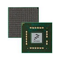
MPC8536DS Freescale Semiconductor, MPC8536DS Datasheet - Page 264

MPC8536DS
Manufacturer Part Number
MPC8536DS
Description
BOARD DEV SYSTEM MPC8536E
Manufacturer
Freescale Semiconductor
Series
PowerQUICC III™r
Type
MPUr
Datasheets
1.MPC8536EBVTAVLA.pdf
(127 pages)
2.MPC8536EBVTAVLA.pdf
(1706 pages)
3.MPC8536DS.pdf
(2 pages)
4.MPC8536DS.pdf
(126 pages)
Specifications of MPC8536DS
Contents
Board, Software and Documentation
Processor Series
MPC85xx
Core
e500
Data Bus Width
32 bit
Maximum Clock Frequency
667 MHz
Operating Supply Voltage
- 0.3 V to + 1.21 V
Maximum Operating Temperature
+ 105 C
Data Ram Size
32 KB
Interface Type
SPI, USB
Program Memory Type
DDR2, DDR3, SDRAM
Core Size
32 Bit
Program Memory Size
544KB
Cpu Speed
1.5GHz
Digital Ic Case Style
BGA
No. Of Pins
783
Supply Voltage Range
0.95V To 1.05V
Rohs Compliant
Yes
For Use With/related Products
MPC8536
Lead Free Status / RoHS Status
Lead free / RoHS Compliant
- MPC8536EBVTAVLA PDF datasheet
- MPC8536EBVTAVLA PDF datasheet #2
- MPC8536DS PDF datasheet #3
- MPC8536DS PDF datasheet #4
- Current page: 264 of 1706
- Download datasheet (15Mb)
e500 Coherency Module
7.1.1
The ECM routes transactions initiated by the e500 core to the appropriate target interface on the device.
In a manner analogous to a bridging router in a local area network, the ECM forwards I/O-initiated
transactions that are tagged with the global attribute onto the core complex bus (CCB). This allows on-chip
caches to snoop these transactions as if they were locally initiated and to take actions to maintain
coherency across cacheable memory.
7.1.2
The ECM includes these distinctive features:
7-2
•
•
•
•
•
•
•
•
•
Support for the e500 core and an L2/SRAM on the CCB, including a CCB arbiter.
It sources a 64-bit data bus for returning read data from the ECM to the e500 core and routing write
data from the ECM to the L2/SRAM. It sinks a 128-bit data bus for receiving data from the
L2/SRAM and a 128-bit write data bus from the e500 core.
Four connection points for I/O initiating (mastering into the device) interfaces. The ECM supports
five connection points for I/O targets. The DDR memory controller, enhanced local bus, OCeaN
targets, and configuration register access block all have a target port connection to the ECM.
Split transaction support—separate address and data tenures allow for pipelining of transactions
and out-of-order data tenures between initiators and targets.
Proper ordering of I/O-initiated transactions.
Speculative read bus for low-latency dispatch of reads to the DDR controller.
Low-latency path for returning read data from DDR to the e500 core.
Error registers trap transactions with invalid addresses. Errors can be programmed to generate
interrupts to the e500 core, as described in the following sections:
—
—
—
—
—
Errors from reading I/O devices terminate with data sent to the master with a corrupt attribute. If
the master is the e500 core, the ECM asserts core_fault_in to the core, which causes the core to
generate a machine check interrupt, unless it is disabled (by clearing HID1[RFXE]). If RFXE is
zero and one of these errors occurs, appropriate interrupts must be enabled to ensure that an
interrupt is generated. See
and the PowerPC™ e500 Core Family Reference Manual.
Section 7.2.1.5, “ECM Error Detect Register (EEDR)”
Section 7.2.1.6, “ECM Error Enable Register (EEER)”
Section 7.2.1.7, “ECM Error Attributes Capture Register (EEATR)”
Section 7.2.1.8, “ECM Error Low Address Capture Register (EELADR)”
Section 7.2.1.9, “ECM Error High Address Capture Register (EEHADR)”
Overview
Features
MPC8536E PowerQUICC III Integrated Processor Reference Manual, Rev. 1
Section 5.2, “e500 Core Integration and the Core Complex Bus
Freescale Semiconductor
(CCB),”
Related parts for MPC8536DS
Image
Part Number
Description
Manufacturer
Datasheet
Request
R
Part Number:
Description:
Manufacturer:
Freescale Semiconductor, Inc
Datasheet:
Part Number:
Description:
Manufacturer:
Freescale Semiconductor, Inc
Datasheet:
Part Number:
Description:
Manufacturer:
Freescale Semiconductor, Inc
Datasheet:
Part Number:
Description:
Manufacturer:
Freescale Semiconductor, Inc
Datasheet:
Part Number:
Description:
Manufacturer:
Freescale Semiconductor, Inc
Datasheet:
Part Number:
Description:
Manufacturer:
Freescale Semiconductor, Inc
Datasheet:
Part Number:
Description:
Manufacturer:
Freescale Semiconductor, Inc
Datasheet:
Part Number:
Description:
Manufacturer:
Freescale Semiconductor, Inc
Datasheet:
Part Number:
Description:
Manufacturer:
Freescale Semiconductor, Inc
Datasheet:
Part Number:
Description:
Manufacturer:
Freescale Semiconductor, Inc
Datasheet:
Part Number:
Description:
Manufacturer:
Freescale Semiconductor, Inc
Datasheet:
Part Number:
Description:
Manufacturer:
Freescale Semiconductor, Inc
Datasheet:
Part Number:
Description:
Manufacturer:
Freescale Semiconductor, Inc
Datasheet:
Part Number:
Description:
Manufacturer:
Freescale Semiconductor, Inc
Datasheet:
Part Number:
Description:
Manufacturer:
Freescale Semiconductor, Inc
Datasheet:


