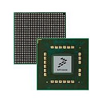
MPC8536DS Freescale Semiconductor, MPC8536DS Datasheet - Page 1087

MPC8536DS
Manufacturer Part Number
MPC8536DS
Description
BOARD DEV SYSTEM MPC8536E
Manufacturer
Freescale Semiconductor
Series
PowerQUICC III™r
Type
MPUr
Datasheets
1.MPC8536EBVTAVLA.pdf
(127 pages)
2.MPC8536EBVTAVLA.pdf
(1706 pages)
3.MPC8536DS.pdf
(2 pages)
4.MPC8536DS.pdf
(126 pages)
Specifications of MPC8536DS
Contents
Board, Software and Documentation
Processor Series
MPC85xx
Core
e500
Data Bus Width
32 bit
Maximum Clock Frequency
667 MHz
Operating Supply Voltage
- 0.3 V to + 1.21 V
Maximum Operating Temperature
+ 105 C
Data Ram Size
32 KB
Interface Type
SPI, USB
Program Memory Type
DDR2, DDR3, SDRAM
Core Size
32 Bit
Program Memory Size
544KB
Cpu Speed
1.5GHz
Digital Ic Case Style
BGA
No. Of Pins
783
Supply Voltage Range
0.95V To 1.05V
Rohs Compliant
Yes
For Use With/related Products
MPC8536
Lead Free Status / RoHS Status
Lead free / RoHS Compliant
- MPC8536EBVTAVLA PDF datasheet
- MPC8536EBVTAVLA PDF datasheet #2
- MPC8536DS PDF datasheet #3
- MPC8536DS PDF datasheet #4
- Current page: 1087 of 1706
- Download datasheet (15Mb)
16.4.2.11.3 Agent Accessing the PCI Configuration Space
When this device is configured as an agent device, it responds to a remote host-generated PCI
configuration cycle. This is indicated by decoding the configuration command along with PCI's IDSEL
being asserted. When the PCI controller detects an access to PCI CFG_DATA, it checks the enable flag
and the device number in the PCI CFG_ADDR register. If the enable bit is set, and the device number is
not 0b1_1111, the PCI controller performs a configuration cycle translation function and runs a
configuration-read or configuration-write transaction on the PCI bus. The device number 0b1_1111 is used
for performing interrupt-acknowledge and special-cycle transactions. See
Transactions,”
0x00), the PCI controller performs a type 0 configuration cycle translation. If the bus number indicates a
remote PCI bus (that is, nonlocal), the PCI controller performs a type 1 configuration cycle translation.
Note that in the following examples, the data in the configuration register is shown in little-endian order.
This is because all the PCI registers are intrinsically little-endian. External PCI masters that use the local
address map to access configuration space do not need to reverse bytes since byte lane redirection from
the little-endian PCI bus is performed internally.
Example: Configuration sequence, 4-byte data write to PCI register at address offset 0x14 of Device 1 on
PCI bus 0.
Initial values:
Code sequence:
Results:
Example: Configuration sequence, 2-byte data write to PCI register at address offset 0x1C of Device 1 on
PCI bus 0.
Initial values:
Code sequence:
Results:
Freescale Semiconductor
r0 contains 0x8000_0814
r1 contains CCSRBAR + BlockBase + 0x000 (Address of PCI CFG_ADDR register)
r2 contains CCSRBAR + BlockBase + 0x004 (Address of PCI CFG_DATA register)
r3 contains 0x1122_3344
Register at 0x14 contains 0xFFFF_FFFF (0x17 to 0x14)
stw r0, 0 (r1) // Update PCI CFG_ADDR register to point to
stwbrx r3, 0 (r2)
Address CCSRBAR + BlockBase + 0x000 contains 0x8000_0814
Register at 0x14 contains 0x1122_3344 (0x17 to 0x14)
r0 contains 0x8000_081C
r1 contains CCSRBAR + BlockBase + 0x000
r2 contains CCSRBAR + BlockBase + 0x004
r3 contains 0xDDCC_BBAA
Register at 0x1C contains 0xFFFF_FFFF (0x1F to 0x1C)
stw r0, 0 (r1)
sthbrx r3, 0 (r2)
Address CCSRBAR + BlockBase + 0x000 contains 0x8000_081C
Register at 0x1C contains 0xFFFF_BBAA (0x1F to 0x1C)
for more information. If the bus number corresponds to the local PCI bus (bus number =
MPC8536E PowerQUICC III Integrated Processor Reference Manual, Rev. 1
//register offset 0x14 of device 1.
Section 16.4.2.12, “Other Bus
PCI Bus Interface
16-61
Related parts for MPC8536DS
Image
Part Number
Description
Manufacturer
Datasheet
Request
R
Part Number:
Description:
Manufacturer:
Freescale Semiconductor, Inc
Datasheet:
Part Number:
Description:
Manufacturer:
Freescale Semiconductor, Inc
Datasheet:
Part Number:
Description:
Manufacturer:
Freescale Semiconductor, Inc
Datasheet:
Part Number:
Description:
Manufacturer:
Freescale Semiconductor, Inc
Datasheet:
Part Number:
Description:
Manufacturer:
Freescale Semiconductor, Inc
Datasheet:
Part Number:
Description:
Manufacturer:
Freescale Semiconductor, Inc
Datasheet:
Part Number:
Description:
Manufacturer:
Freescale Semiconductor, Inc
Datasheet:
Part Number:
Description:
Manufacturer:
Freescale Semiconductor, Inc
Datasheet:
Part Number:
Description:
Manufacturer:
Freescale Semiconductor, Inc
Datasheet:
Part Number:
Description:
Manufacturer:
Freescale Semiconductor, Inc
Datasheet:
Part Number:
Description:
Manufacturer:
Freescale Semiconductor, Inc
Datasheet:
Part Number:
Description:
Manufacturer:
Freescale Semiconductor, Inc
Datasheet:
Part Number:
Description:
Manufacturer:
Freescale Semiconductor, Inc
Datasheet:
Part Number:
Description:
Manufacturer:
Freescale Semiconductor, Inc
Datasheet:
Part Number:
Description:
Manufacturer:
Freescale Semiconductor, Inc
Datasheet:


