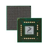
MPC8536DS Freescale Semiconductor, MPC8536DS Datasheet - Page 1238

MPC8536DS
Manufacturer Part Number
MPC8536DS
Description
BOARD DEV SYSTEM MPC8536E
Manufacturer
Freescale Semiconductor
Series
PowerQUICC III™r
Type
MPUr
Datasheets
1.MPC8536EBVTAVLA.pdf
(127 pages)
2.MPC8536EBVTAVLA.pdf
(1706 pages)
3.MPC8536DS.pdf
(2 pages)
4.MPC8536DS.pdf
(126 pages)
Specifications of MPC8536DS
Contents
Board, Software and Documentation
Processor Series
MPC85xx
Core
e500
Data Bus Width
32 bit
Maximum Clock Frequency
667 MHz
Operating Supply Voltage
- 0.3 V to + 1.21 V
Maximum Operating Temperature
+ 105 C
Data Ram Size
32 KB
Interface Type
SPI, USB
Program Memory Type
DDR2, DDR3, SDRAM
Core Size
32 Bit
Program Memory Size
544KB
Cpu Speed
1.5GHz
Digital Ic Case Style
BGA
No. Of Pins
783
Supply Voltage Range
0.95V To 1.05V
Rohs Compliant
Yes
For Use With/related Products
MPC8536
Lead Free Status / RoHS Status
Lead free / RoHS Compliant
- MPC8536EBVTAVLA PDF datasheet
- MPC8536EBVTAVLA PDF datasheet #2
- MPC8536DS PDF datasheet #3
- MPC8536DS PDF datasheet #4
- Current page: 1238 of 1706
- Download datasheet (15Mb)
SATA Controller
Figure 19-5
19.3.2.5
When a single device error is detected, the device that issued the error is indicated by the hardware setting
the device error bit to a 1 in the DER (shown in
error register applies to the queues and to restarting the device.
The host application software acknowledges the device in error by clearing the device error bit. The device
error is cleared by writing a 1 to the appropriate device error bit. When this action is performed, the queue
to the device in error is cleared and is ready to have commands queue.
While a device is in error, no command can be queued for that device.
Table 19-6
19.3.2.6
The CHBA is shown in
block is located. It must be written as part of the host software initialization process. After the SATA
controller hardware is brought online, the SATA controller takes ownership of this register. The address in
this register should not be changed while the SATA controller is online.
19-8
Offset 0x1_8020
Reset
Offset 0x1_8024
Reset
W
W
R
R
31
31
describes the DER fields.
describes the CER fields.
Device Error Register (DER)
Command Header Base Address Register (CHBA)
MPC8536E PowerQUICC III Integrated Processor Reference Manual, Rev. 1
Figure 19-7. Command Header Base Address Register (CHBA)
Figure
31–16
31–16
31–0
15–0
Bit
Bit
—
19-7. This holds the address in memory of where the command header
Figure 19-6. Device Error Register (DER)
Table 19-5. CER Field Descriptions
Table 19-6. DER Field Descriptions
Name
Name
CE n
DE n
—
—
Command Header Base
Figure
Reserved
Command n error bit
Reserved
Device n error bit
All zeros
All zeros
16 15
19-6). The procedure as outlined in the command
Description
Description
DE n
Freescale Semiconductor
Access: Read/Write
Access: w1c
2
1
—
0
0
Related parts for MPC8536DS
Image
Part Number
Description
Manufacturer
Datasheet
Request
R
Part Number:
Description:
Manufacturer:
Freescale Semiconductor, Inc
Datasheet:
Part Number:
Description:
Manufacturer:
Freescale Semiconductor, Inc
Datasheet:
Part Number:
Description:
Manufacturer:
Freescale Semiconductor, Inc
Datasheet:
Part Number:
Description:
Manufacturer:
Freescale Semiconductor, Inc
Datasheet:
Part Number:
Description:
Manufacturer:
Freescale Semiconductor, Inc
Datasheet:
Part Number:
Description:
Manufacturer:
Freescale Semiconductor, Inc
Datasheet:
Part Number:
Description:
Manufacturer:
Freescale Semiconductor, Inc
Datasheet:
Part Number:
Description:
Manufacturer:
Freescale Semiconductor, Inc
Datasheet:
Part Number:
Description:
Manufacturer:
Freescale Semiconductor, Inc
Datasheet:
Part Number:
Description:
Manufacturer:
Freescale Semiconductor, Inc
Datasheet:
Part Number:
Description:
Manufacturer:
Freescale Semiconductor, Inc
Datasheet:
Part Number:
Description:
Manufacturer:
Freescale Semiconductor, Inc
Datasheet:
Part Number:
Description:
Manufacturer:
Freescale Semiconductor, Inc
Datasheet:
Part Number:
Description:
Manufacturer:
Freescale Semiconductor, Inc
Datasheet:
Part Number:
Description:
Manufacturer:
Freescale Semiconductor, Inc
Datasheet:


