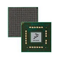
MPC8536DS Freescale Semiconductor, MPC8536DS Datasheet - Page 1071

MPC8536DS
Manufacturer Part Number
MPC8536DS
Description
BOARD DEV SYSTEM MPC8536E
Manufacturer
Freescale Semiconductor
Series
PowerQUICC III™r
Type
MPUr
Datasheets
1.MPC8536EBVTAVLA.pdf
(127 pages)
2.MPC8536EBVTAVLA.pdf
(1706 pages)
3.MPC8536DS.pdf
(2 pages)
4.MPC8536DS.pdf
(126 pages)
Specifications of MPC8536DS
Contents
Board, Software and Documentation
Processor Series
MPC85xx
Core
e500
Data Bus Width
32 bit
Maximum Clock Frequency
667 MHz
Operating Supply Voltage
- 0.3 V to + 1.21 V
Maximum Operating Temperature
+ 105 C
Data Ram Size
32 KB
Interface Type
SPI, USB
Program Memory Type
DDR2, DDR3, SDRAM
Core Size
32 Bit
Program Memory Size
544KB
Cpu Speed
1.5GHz
Digital Ic Case Style
BGA
No. Of Pins
783
Supply Voltage Range
0.95V To 1.05V
Rohs Compliant
Yes
For Use With/related Products
MPC8536
Lead Free Status / RoHS Status
Lead free / RoHS Compliant
- MPC8536EBVTAVLA PDF datasheet
- MPC8536EBVTAVLA PDF datasheet #2
- MPC8536DS PDF datasheet #3
- MPC8536DS PDF datasheet #4
- Current page: 1071 of 1706
- Download datasheet (15Mb)
REQ is negated for at least one clock cycle. This prevents ill-behaved masters from monopolizing the bus.
When the broken master feature is disabled, a device that requests the bus and receives a grant never loses
its grant until and unless it begins a transaction or negates its REQ signal. Note that disabling the broken
master feature is not recommended.
16.4.1.4
In the sleep power-saving mode, the clock signal driving SYSCLK can be disabled. If the clock is disabled,
the arbitration logic is not able to perform its function. System programmers must park the bus with a
device that can sustain the PCI_AD[31:0], PCI_C/BE[3:0], and parity signals prior to disabling the
SYSCLK signal. If the bus is parked on the MPC8536E when its clocks are stopped, the MPC8536E
sustains the PCI_AD[31:0], PCI_C/BE[3:0], and parity signals in their prior states. In this situation, the
only way for another agent to use the PCI bus is by waking the MPC8536E. In nap and doze power-saving
modes, the arbiter continues to operate allowing other PCI devices to run transactions.
16.4.2
This section provides a general description of the PCI bus protocol. Specific PCI bus transactions are
described in
and
All signals are sampled on the rising edge of the PCI bus clock (SYSCLK). Each signal has a setup and
hold aperture with respect to the rising clock edge in which transitions are not allowed. Outside this
aperture, signal values or transitions have no significance. See the separate hardware specifications
document for specific setup and hold times.
16.4.2.1
The basic PCI bus transfer mechanism is a burst. A burst is composed of an address phase followed by one
or more data phases. Fundamentally, all PCI data transfers are controlled by three signals—PCI_FRAME
(frame), PCI_IRDY (initiator ready), and PCI_TRDY (target ready). An initiator asserts PCI_FRAME to
indicate the beginning of a PCI bus transaction and negates PCI_FRAME to indicate the end of a PCI bus
transaction. An initiator negates PCI_IRDY to force wait cycles. A target negates PCI_TRDY to force wait
cycles.
The PCI bus is considered idle when both PCI_FRAME and PCI_IRDY are negated. The first clock cycle
in which PCI_FRAME is asserted indicates the beginning of the address phase. The address and bus
command code are transferred in that first cycle. The next cycle begins the first of one or more data phases.
Data is transferred between initiator and target in each cycle that both PCI_IRDY and PCI_TRDY are
asserted. Wait cycles may be inserted in a data phase by the initiator (by negating PCI_IRDY) or by the
target (by negating PCI_TRDY).
Once an initiator has asserted PCI_IRDY, it cannot change PCI_IRDY or PCI_FRAME until the current
data phase completes regardless of the state of PCI_TRDY. Once a target has asserted PCI_TRDY or
PCI_STOP, it cannot change PCI_DEVSEL, PCI_TRDY, or PCI_STOP until the current data phase
completes. In simpler terms, once an initiator or target has committed to the data transfer, it cannot change
its mind.
Freescale Semiconductor
Figure 16-52
PCI Bus Protocol
Section 16.4.2.7, “PCI Bus Transactions.”
Power-Saving Modes and the PCI Arbiter
Basic Transfer Control
for examples of the transfer-control mechanisms described in this section.
MPC8536E PowerQUICC III Integrated Processor Reference Manual, Rev. 1
Refer to
Figure
16-49,
Figure
16-50,
Figure
PCI Bus Interface
16-51,
16-45
Related parts for MPC8536DS
Image
Part Number
Description
Manufacturer
Datasheet
Request
R
Part Number:
Description:
Manufacturer:
Freescale Semiconductor, Inc
Datasheet:
Part Number:
Description:
Manufacturer:
Freescale Semiconductor, Inc
Datasheet:
Part Number:
Description:
Manufacturer:
Freescale Semiconductor, Inc
Datasheet:
Part Number:
Description:
Manufacturer:
Freescale Semiconductor, Inc
Datasheet:
Part Number:
Description:
Manufacturer:
Freescale Semiconductor, Inc
Datasheet:
Part Number:
Description:
Manufacturer:
Freescale Semiconductor, Inc
Datasheet:
Part Number:
Description:
Manufacturer:
Freescale Semiconductor, Inc
Datasheet:
Part Number:
Description:
Manufacturer:
Freescale Semiconductor, Inc
Datasheet:
Part Number:
Description:
Manufacturer:
Freescale Semiconductor, Inc
Datasheet:
Part Number:
Description:
Manufacturer:
Freescale Semiconductor, Inc
Datasheet:
Part Number:
Description:
Manufacturer:
Freescale Semiconductor, Inc
Datasheet:
Part Number:
Description:
Manufacturer:
Freescale Semiconductor, Inc
Datasheet:
Part Number:
Description:
Manufacturer:
Freescale Semiconductor, Inc
Datasheet:
Part Number:
Description:
Manufacturer:
Freescale Semiconductor, Inc
Datasheet:
Part Number:
Description:
Manufacturer:
Freescale Semiconductor, Inc
Datasheet:


