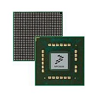
MPC8536DS Freescale Semiconductor, MPC8536DS Datasheet - Page 251

MPC8536DS
Manufacturer Part Number
MPC8536DS
Description
BOARD DEV SYSTEM MPC8536E
Manufacturer
Freescale Semiconductor
Series
PowerQUICC III™r
Type
MPUr
Datasheets
1.MPC8536EBVTAVLA.pdf
(127 pages)
2.MPC8536EBVTAVLA.pdf
(1706 pages)
3.MPC8536DS.pdf
(2 pages)
4.MPC8536DS.pdf
(126 pages)
Specifications of MPC8536DS
Contents
Board, Software and Documentation
Processor Series
MPC85xx
Core
e500
Data Bus Width
32 bit
Maximum Clock Frequency
667 MHz
Operating Supply Voltage
- 0.3 V to + 1.21 V
Maximum Operating Temperature
+ 105 C
Data Ram Size
32 KB
Interface Type
SPI, USB
Program Memory Type
DDR2, DDR3, SDRAM
Core Size
32 Bit
Program Memory Size
544KB
Cpu Speed
1.5GHz
Digital Ic Case Style
BGA
No. Of Pins
783
Supply Voltage Range
0.95V To 1.05V
Rohs Compliant
Yes
For Use With/related Products
MPC8536
Lead Free Status / RoHS Status
Lead free / RoHS Compliant
- MPC8536EBVTAVLA PDF datasheet
- MPC8536EBVTAVLA PDF datasheet #2
- MPC8536DS PDF datasheet #3
- MPC8536DS PDF datasheet #4
- Current page: 251 of 1706
- Download datasheet (15Mb)
6.7.5
Locks for instructions and data are recorded separately in the L2 cache, and they can be flash cleared
separately by writing the appropriate value to the L2 cache control register (L2CTL[L2LFR] and
L2CTL[L2LFRID]). Flash invalidating of the L2 (setting L2CTL[L2I]) clears all locks on both
instructions and data.
Note that flash clearing is the only way to clear data locks without clearing instruction locks, or to clear
instruction locks without clearing data locks. All instructions and snoop transactions that clear locks clear
both data and instruction locks.
6.7.6
If data is locked in the L2 and either the e500 core performs a cacheable copyback store or a dcbtst misses
in the L1, the L2 invalidates the line; however, the L2 clears the valid bit for the data, the lock remains,
and the line cannot be victimized. If the e500 core casts out modified data or pushes it in response to a
non-flush snoop, the L2 updates the data and sets the valid bit again, maintaining the lock and keeping the
data in the cache hierarchy.
6.8
Line replacement is determined using a pseudo least-recently-used (PLRU) algorithm. There is a valid bit
(V0–V7) for each line. To determine the replacement victim (the line to be cast out), there are seven PLRU
bits (P0–P6) for each set. PLRU bits are updated every time a new line is allocated and every time an
existing line is read by the processor, updated by a write, or invalidated.
Figure 6-26
are labeled W0–W7; the seven PLRU bits are labeled P0–P6.
Freescale Semiconductor
PLRU L2 Replacement Policy
shows the binary decision tree used to generate the victim line. The eight ways of the L2 cache
Flash Clearing of Instruction and Data Locks
Locks with Stale Data
MPC8536E PowerQUICC III Integrated Processor Reference Manual, Rev. 1
P0
P1
P2
P3
P4
P5
P6
Allocate
Yes
W0
Figure 6-26. L2 Cache Line Replacement Algorithm
0
0
x
0
x
x
x
P3 = 0?
Allocate
Yes
W1
No
0
0
x
1
x
x
x
P1 = 0?
Allocate
W2
Yes
0
1
0
x
x
x
x
P4 = 0?
Yes
No
Allocate
W3
0
1
1
No
x
x
x
x
P0 = 0?
Allocate
Yes
W4
P5 = 0?
1
0
0
x
x
x
x
No
Yes
Allocate
No
W5
1
0
1
x
x
x
x
P2 = 0?
Allocate
Yes
W6
1
x
1
x
x
x
0
P6 = 0?
No
Allocate
W7
No
1
x
1
x
x
x
1
L2 Look-Aside Cache/SRAM
6-31
Related parts for MPC8536DS
Image
Part Number
Description
Manufacturer
Datasheet
Request
R
Part Number:
Description:
Manufacturer:
Freescale Semiconductor, Inc
Datasheet:
Part Number:
Description:
Manufacturer:
Freescale Semiconductor, Inc
Datasheet:
Part Number:
Description:
Manufacturer:
Freescale Semiconductor, Inc
Datasheet:
Part Number:
Description:
Manufacturer:
Freescale Semiconductor, Inc
Datasheet:
Part Number:
Description:
Manufacturer:
Freescale Semiconductor, Inc
Datasheet:
Part Number:
Description:
Manufacturer:
Freescale Semiconductor, Inc
Datasheet:
Part Number:
Description:
Manufacturer:
Freescale Semiconductor, Inc
Datasheet:
Part Number:
Description:
Manufacturer:
Freescale Semiconductor, Inc
Datasheet:
Part Number:
Description:
Manufacturer:
Freescale Semiconductor, Inc
Datasheet:
Part Number:
Description:
Manufacturer:
Freescale Semiconductor, Inc
Datasheet:
Part Number:
Description:
Manufacturer:
Freescale Semiconductor, Inc
Datasheet:
Part Number:
Description:
Manufacturer:
Freescale Semiconductor, Inc
Datasheet:
Part Number:
Description:
Manufacturer:
Freescale Semiconductor, Inc
Datasheet:
Part Number:
Description:
Manufacturer:
Freescale Semiconductor, Inc
Datasheet:
Part Number:
Description:
Manufacturer:
Freescale Semiconductor, Inc
Datasheet:


