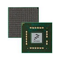
MPC8536DS Freescale Semiconductor, MPC8536DS Datasheet - Page 291

MPC8536DS
Manufacturer Part Number
MPC8536DS
Description
BOARD DEV SYSTEM MPC8536E
Manufacturer
Freescale Semiconductor
Series
PowerQUICC III™r
Type
MPUr
Datasheets
1.MPC8536EBVTAVLA.pdf
(127 pages)
2.MPC8536EBVTAVLA.pdf
(1706 pages)
3.MPC8536DS.pdf
(2 pages)
4.MPC8536DS.pdf
(126 pages)
Specifications of MPC8536DS
Contents
Board, Software and Documentation
Processor Series
MPC85xx
Core
e500
Data Bus Width
32 bit
Maximum Clock Frequency
667 MHz
Operating Supply Voltage
- 0.3 V to + 1.21 V
Maximum Operating Temperature
+ 105 C
Data Ram Size
32 KB
Interface Type
SPI, USB
Program Memory Type
DDR2, DDR3, SDRAM
Core Size
32 Bit
Program Memory Size
544KB
Cpu Speed
1.5GHz
Digital Ic Case Style
BGA
No. Of Pins
783
Supply Voltage Range
0.95V To 1.05V
Rohs Compliant
Yes
For Use With/related Products
MPC8536
Lead Free Status / RoHS Status
Lead free / RoHS Compliant
- MPC8536EBVTAVLA PDF datasheet
- MPC8536EBVTAVLA PDF datasheet #2
- MPC8536DS PDF datasheet #3
- MPC8536DS PDF datasheet #4
- Current page: 291 of 1706
- Download datasheet (15Mb)
8.4.1.5
DDR SDRAM timing configuration register 0, shown in
between various SDRAM control commands.
Freescale Semiconductor
20–28
29–31
Offset 0x104
Reset 0 0
Bits
19
W
R
RWT WRT RRT
0
EXT_CASLAT
1
CNTL_ADJ
Name
0 0 0
2
DDR SDRAM Timing Configuration 0 (TIMING_CFG_0)
—
3 4
MPC8536E PowerQUICC III Integrated Processor Reference Manual, Rev. 1
Figure 8-6. DDR SDRAM Timing Configuration 0 (TIMING_CFG_0)
0
5
Extended MCAS latency from READ command. Number of clock cycles between registration of a
READ command by the SDRAM and the availability of the first output data. If a READ command is
registered at clock edge
clock edge
for the total CAS latency. Note that if this bit is set, then 8 clocks are added to the programmed value
in TIMING_CFG_1[CASLAT].
0
Reserved, should be cleared.
Control Adjust. Controls the amount of delay to add to the lightly loaded control signals w/ respect to
all other DRAM address and command signals. The signals affected by this field are MODT[0:3],
MCS[0:3], and MCKE[0:3]
000 MODT[0:3], MCS[0:3], and MCKE[0:3] are launched aligned with the other DRAM address and
001 MODT[0:3], MCS[0:3], and MCKE[0:3] are launched 1/2 platform cycle later than the other
010 MODT[0:3], MCS[0:3], and MCKE[0:3] are launched 1 platform cycle later than the other
011 MODT[0:3], MCS[0:3], and MCKE[0:3] are launched 3/2 platform cycles later than the other
100 MODT[0:3], MCS[0:3], and MCKE[0:3] are launched 2 platform cycles later than the other
101 MODT[0:3], MCS[0:3], and MCKE[0:3] are launched 5/2 platform cycles later than the other
110-111Reserved
WWT — ACT_PD_EXIT
0
6
Table 8-9. TIMING_CFG_3 Field Descriptions (continued)
0
7
0 clocks
control signals.
DRAM address and control signals.
DRAM address and control signals.
DRAM address and control signals.
DRAM address and control signals.
DRAM address and control signals.
8
0
n
0
+
9
m
. This field is concatenated with TIMING_CFG_1[CASLAT] to obtain a 5-bit value
0
11
1
n
and the latency is
12
0
PRE_PD_EXIT
0
0
Figure
Description
15
m
1
clocks, data is available nominally coincident with
16
0 0 0 0
8-6, sets the number of clock cycles
1
—
8 clocks
19 20
ODT_PD_EXIT
0
0
0
23 24
1
DDR Memory Controller
0 0 0 0 0 1 0 1
Access: Read/Write
—
27 28
MRS_CYC
8-17
31
Related parts for MPC8536DS
Image
Part Number
Description
Manufacturer
Datasheet
Request
R
Part Number:
Description:
Manufacturer:
Freescale Semiconductor, Inc
Datasheet:
Part Number:
Description:
Manufacturer:
Freescale Semiconductor, Inc
Datasheet:
Part Number:
Description:
Manufacturer:
Freescale Semiconductor, Inc
Datasheet:
Part Number:
Description:
Manufacturer:
Freescale Semiconductor, Inc
Datasheet:
Part Number:
Description:
Manufacturer:
Freescale Semiconductor, Inc
Datasheet:
Part Number:
Description:
Manufacturer:
Freescale Semiconductor, Inc
Datasheet:
Part Number:
Description:
Manufacturer:
Freescale Semiconductor, Inc
Datasheet:
Part Number:
Description:
Manufacturer:
Freescale Semiconductor, Inc
Datasheet:
Part Number:
Description:
Manufacturer:
Freescale Semiconductor, Inc
Datasheet:
Part Number:
Description:
Manufacturer:
Freescale Semiconductor, Inc
Datasheet:
Part Number:
Description:
Manufacturer:
Freescale Semiconductor, Inc
Datasheet:
Part Number:
Description:
Manufacturer:
Freescale Semiconductor, Inc
Datasheet:
Part Number:
Description:
Manufacturer:
Freescale Semiconductor, Inc
Datasheet:
Part Number:
Description:
Manufacturer:
Freescale Semiconductor, Inc
Datasheet:
Part Number:
Description:
Manufacturer:
Freescale Semiconductor, Inc
Datasheet:


