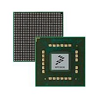
MPC8536DS Freescale Semiconductor, MPC8536DS Datasheet - Page 762

MPC8536DS
Manufacturer Part Number
MPC8536DS
Description
BOARD DEV SYSTEM MPC8536E
Manufacturer
Freescale Semiconductor
Series
PowerQUICC III™r
Type
MPUr
Datasheets
1.MPC8536EBVTAVLA.pdf
(127 pages)
2.MPC8536EBVTAVLA.pdf
(1706 pages)
3.MPC8536DS.pdf
(2 pages)
4.MPC8536DS.pdf
(126 pages)
Specifications of MPC8536DS
Contents
Board, Software and Documentation
Processor Series
MPC85xx
Core
e500
Data Bus Width
32 bit
Maximum Clock Frequency
667 MHz
Operating Supply Voltage
- 0.3 V to + 1.21 V
Maximum Operating Temperature
+ 105 C
Data Ram Size
32 KB
Interface Type
SPI, USB
Program Memory Type
DDR2, DDR3, SDRAM
Core Size
32 Bit
Program Memory Size
544KB
Cpu Speed
1.5GHz
Digital Ic Case Style
BGA
No. Of Pins
783
Supply Voltage Range
0.95V To 1.05V
Rohs Compliant
Yes
For Use With/related Products
MPC8536
Lead Free Status / RoHS Status
Lead free / RoHS Compliant
- MPC8536EBVTAVLA PDF datasheet
- MPC8536EBVTAVLA PDF datasheet #2
- MPC8536DS PDF datasheet #3
- MPC8536DS PDF datasheet #4
- Current page: 762 of 1706
- Download datasheet (15Mb)
Enhanced Three-Speed Ethernet Controllers
14.5
The eTSECs use a software model that is a superset of the PowerQUICC III TSEC functionality and is
similar to that employed by the Fast Ethernet function supported on the Freescale MPC8260 CPM FCC
and in the FEC of the MPC860T.
The eTSEC device is programmed by a combination of control/status registers (CSRs) and buffer
descriptors. The CSRs are used for mode control, interrupts, and to extract status information. The
descriptors are used to pass data buffers and related buffer status or frame information between the
hardware and software.
All accesses to and from the registers must be made as 32-bit accesses. There is no support for accesses of
sizes other than 32 bits. Writes to reserved register bits must always store 0, as writing 1 to reserved bits
may have unintended side-effects. Reads from unmapped register addresses return zero. Unless otherwise
specified, the read value of reserved bits in mapped registers is not defined, and must not be assumed to
be 0.
This section of the document defines the memory map and describes the registers in detail. The buffer
descriptor is described in
The ten-bit interface (TBI) and reduced ten-bit interface (RTBI) module MII registers are also described
in this section. The TBI/RTBI registers are defined like PHY registers and, as such, are accessed through
the MII management interface in the same way the PHYs are accessed. For detailed descriptions of the
TBI/RTBI registers (the MII register set for the ten-bit interface) refer to
(TBI).”
14-14
SD2_REF_CLK
SD2_REF_CLK
TSEC_1588_
TSEC_1588_
SD2_TX[0:1]
SD2_TX[0:1]
SD2_RX[0:1]
SD2_RX[0:1]
TRIG_OUT0
TRIG_OUT1
Signal
Memory Map/Register Definition
Table 14-2. eTSEC Signals—Detailed Signal Descriptions (continued)
MPC8536E PowerQUICC III Integrated Processor Reference Manual, Rev. 1
I/O
O
O
O
I
I
1588 timer alarm 0. Timer current time is equal to or greater than alarm time comparator register.
User reprograms the TSEC_1588_ALARM n _H/L register to deactivate this output (chip external
output pin)
1588 timer alarm 1. Timer current time is equal to or greater than alarm time comparator register.
User reprograms the TSEC_1588_ALARM n _H/L register to deactivate this output (chip external
output pin)
SGMII transmit data (and complement)
When in SGMII interface mode:
SGMII receive data (and complement)
When in SGMII interface mode:
SGMII SerDes2 PLL reference clock (and complement)
Section 14.6.8, “Buffer Descriptors.”
• eTSEC1 utilizes SD2_TX[0] and SD2_TX[0]
• eTSEC3 utilizes SD2_TX[2] and SD2_TX[2]
• eTSEC1 utilizes SD2_RX[0] and SD2_RX[0]
• eTSEC3 utilizes SD2_RX[2] and SD2_RX[2]
Description
Section 14.5.4, “Ten-Bit Interface
Freescale Semiconductor
Related parts for MPC8536DS
Image
Part Number
Description
Manufacturer
Datasheet
Request
R
Part Number:
Description:
Manufacturer:
Freescale Semiconductor, Inc
Datasheet:
Part Number:
Description:
Manufacturer:
Freescale Semiconductor, Inc
Datasheet:
Part Number:
Description:
Manufacturer:
Freescale Semiconductor, Inc
Datasheet:
Part Number:
Description:
Manufacturer:
Freescale Semiconductor, Inc
Datasheet:
Part Number:
Description:
Manufacturer:
Freescale Semiconductor, Inc
Datasheet:
Part Number:
Description:
Manufacturer:
Freescale Semiconductor, Inc
Datasheet:
Part Number:
Description:
Manufacturer:
Freescale Semiconductor, Inc
Datasheet:
Part Number:
Description:
Manufacturer:
Freescale Semiconductor, Inc
Datasheet:
Part Number:
Description:
Manufacturer:
Freescale Semiconductor, Inc
Datasheet:
Part Number:
Description:
Manufacturer:
Freescale Semiconductor, Inc
Datasheet:
Part Number:
Description:
Manufacturer:
Freescale Semiconductor, Inc
Datasheet:
Part Number:
Description:
Manufacturer:
Freescale Semiconductor, Inc
Datasheet:
Part Number:
Description:
Manufacturer:
Freescale Semiconductor, Inc
Datasheet:
Part Number:
Description:
Manufacturer:
Freescale Semiconductor, Inc
Datasheet:
Part Number:
Description:
Manufacturer:
Freescale Semiconductor, Inc
Datasheet:


