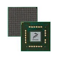
MPC8536DS Freescale Semiconductor, MPC8536DS Datasheet - Page 737

MPC8536DS
Manufacturer Part Number
MPC8536DS
Description
BOARD DEV SYSTEM MPC8536E
Manufacturer
Freescale Semiconductor
Series
PowerQUICC III™r
Type
MPUr
Datasheets
1.MPC8536EBVTAVLA.pdf
(127 pages)
2.MPC8536EBVTAVLA.pdf
(1706 pages)
3.MPC8536DS.pdf
(2 pages)
4.MPC8536DS.pdf
(126 pages)
Specifications of MPC8536DS
Contents
Board, Software and Documentation
Processor Series
MPC85xx
Core
e500
Data Bus Width
32 bit
Maximum Clock Frequency
667 MHz
Operating Supply Voltage
- 0.3 V to + 1.21 V
Maximum Operating Temperature
+ 105 C
Data Ram Size
32 KB
Interface Type
SPI, USB
Program Memory Type
DDR2, DDR3, SDRAM
Core Size
32 Bit
Program Memory Size
544KB
Cpu Speed
1.5GHz
Digital Ic Case Style
BGA
No. Of Pins
783
Supply Voltage Range
0.95V To 1.05V
Rohs Compliant
Yes
For Use With/related Products
MPC8536
Lead Free Status / RoHS Status
Lead free / RoHS Compliant
- MPC8536EBVTAVLA PDF datasheet
- MPC8536EBVTAVLA PDF datasheet #2
- MPC8536DS PDF datasheet #3
- MPC8536DS PDF datasheet #4
- Current page: 737 of 1706
- Download datasheet (15Mb)
13.5.4
In order to program the eLBC and FCM for executing NAND Flash command sequences, command codes
and pause states should be obtained from the relevant NAND Flash device data sheet and programmed into
FCM configuration registers. This section illustrates some common sequences for large-page,
multi-gigabit NAND Flash EEPROMs; however, details should be verified against manufacturers’
specific programming data.
Throughout these examples it is assumed that one or more banks of eLBC has been configured under FCM
control (BRn[MSEL] = 001), with base address, port size, ECC mode, and timing parameters configured
in accordance with the device’s hardware specifications.
13.5.4.1
An example of configuring FCM to execute a soft reset command to large-page NAND Flash is shown in
Table
by writing FMR[OP] = 10, and issuing a special operation to the bank. At the conclusion of the sequence,
eLBC will issue a command complete interrupt (LTESR[CC]) if interrupts are enabled.
Freescale Semiconductor
1
2
3
Address state is the calculated address for port size.
OP n : These lanes are read or written during that bus transaction. OP0 is the most-significant byte of a doubleword
— Denotes a byte not driven during that read cycle.
operand and OP7 is the least-significant byte.
Half Word
Transfer
Word
Size
13-44. This sequence does not require use of the shared FCM buffer RAM. The sequence is initiated
Register
Command Sequence Examples for NAND Flash EEPROM
FBAR
NAND Flash Soft Reset Command Sequence Example
FCR
Address
State
3 lsbs
000
001
010
100
101
110
000
100
Table 13-43. Data Bus Drive Requirements For Read Cycles (continued)
MPC8536E PowerQUICC III Integrated Processor Reference Manual, Rev. 1
Table 13-44. FCM Register Settings for Soft Reset (OR n [PGS] = 1)
1
Initial Contents
OP0
OP4
OP0
OP4
0–7
—
—
—
—
0xFF000000
—
8–15
OP1
OP1
OP5
OP5
OP1
OP5
—
—
32-Bit
16–23 24–31
OP2
OP2
OP6
OP6
OP2
OP6
—
—
CMD0 = 0xFF = reset command; other commands unused
unused
OP3
OP7
OP3
OP7
—
—
—
—
Port Size/LAD Data Bus Assignments
OP0
OP2
OP4
OP6
OP0
OP4
0–7
—
—
8–15
OP1
OP1
OP3
OP5
OP5
OP7
OP1
OP5
16-Bit
Description
16–23 24–31
OP0
OP1
OP2
OP4
OP5
OP6
OP0
OP4
0–7
Enhanced Local Bus Controller
8–15
8-Bit
16–23 24–31
13-95
Related parts for MPC8536DS
Image
Part Number
Description
Manufacturer
Datasheet
Request
R
Part Number:
Description:
Manufacturer:
Freescale Semiconductor, Inc
Datasheet:
Part Number:
Description:
Manufacturer:
Freescale Semiconductor, Inc
Datasheet:
Part Number:
Description:
Manufacturer:
Freescale Semiconductor, Inc
Datasheet:
Part Number:
Description:
Manufacturer:
Freescale Semiconductor, Inc
Datasheet:
Part Number:
Description:
Manufacturer:
Freescale Semiconductor, Inc
Datasheet:
Part Number:
Description:
Manufacturer:
Freescale Semiconductor, Inc
Datasheet:
Part Number:
Description:
Manufacturer:
Freescale Semiconductor, Inc
Datasheet:
Part Number:
Description:
Manufacturer:
Freescale Semiconductor, Inc
Datasheet:
Part Number:
Description:
Manufacturer:
Freescale Semiconductor, Inc
Datasheet:
Part Number:
Description:
Manufacturer:
Freescale Semiconductor, Inc
Datasheet:
Part Number:
Description:
Manufacturer:
Freescale Semiconductor, Inc
Datasheet:
Part Number:
Description:
Manufacturer:
Freescale Semiconductor, Inc
Datasheet:
Part Number:
Description:
Manufacturer:
Freescale Semiconductor, Inc
Datasheet:
Part Number:
Description:
Manufacturer:
Freescale Semiconductor, Inc
Datasheet:
Part Number:
Description:
Manufacturer:
Freescale Semiconductor, Inc
Datasheet:


