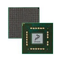
MPC8536DS Freescale Semiconductor, MPC8536DS Datasheet - Page 645

MPC8536DS
Manufacturer Part Number
MPC8536DS
Description
BOARD DEV SYSTEM MPC8536E
Manufacturer
Freescale Semiconductor
Series
PowerQUICC III™r
Type
MPUr
Datasheets
1.MPC8536EBVTAVLA.pdf
(127 pages)
2.MPC8536EBVTAVLA.pdf
(1706 pages)
3.MPC8536DS.pdf
(2 pages)
4.MPC8536DS.pdf
(126 pages)
Specifications of MPC8536DS
Contents
Board, Software and Documentation
Processor Series
MPC85xx
Core
e500
Data Bus Width
32 bit
Maximum Clock Frequency
667 MHz
Operating Supply Voltage
- 0.3 V to + 1.21 V
Maximum Operating Temperature
+ 105 C
Data Ram Size
32 KB
Interface Type
SPI, USB
Program Memory Type
DDR2, DDR3, SDRAM
Core Size
32 Bit
Program Memory Size
544KB
Cpu Speed
1.5GHz
Digital Ic Case Style
BGA
No. Of Pins
783
Supply Voltage Range
0.95V To 1.05V
Rohs Compliant
Yes
For Use With/related Products
MPC8536
Lead Free Status / RoHS Status
Lead free / RoHS Compliant
- MPC8536EBVTAVLA PDF datasheet
- MPC8536EBVTAVLA PDF datasheet #2
- MPC8536DS PDF datasheet #3
- MPC8536DS PDF datasheet #4
- Current page: 645 of 1706
- Download datasheet (15Mb)
13.1.3
The eLBC provides one GPCM, one FCM, and three UPMs for the local bus, with no restriction on how
many of the eight banks (chip selects) can be programmed to operate with any given machine. The internal
transaction address is limited to 32 bits, so all chip selects must fall within the 4-Gbyte window addressed
by the internal transaction address. When a memory transaction is dispatched to the eLBC, the internal
transaction address is compared with the address information of each bank (chip select). The
corresponding machine assigned to that bank (GPCM, FCM, or UPM) then takes ownership of the external
signals that control the access and maintains control until the transaction ends. Thus, with the eLBC in
GPCM or FCM, or UPM mode, only one of the eight chip selects is active at any time for the duration of
the transaction except in the case of UPM refresh where all UPM machines that are enabled for refresh
have concurrent chip select assertion.
Freescale Semiconductor
•
•
•
— Read-only ECC registers to verify after write operation
— Boot chip-select support for 8-bit devices
— Dual 2-Kbyte/eight 512-byte buffers allow simultaneous data transfer during flash reads and
— Interrupt-driven block transfer for reads and writes
— Programmable command and data transfer sequences of up to eight steps supported
— Generic command and address registers support proprietary flash interfaces
— Block write locking to ensure system security and integrity
Three user-programmable machines (UPMs)
— Programmable-array-based machine controls external signal timing with a granularity of up to
— User-specified control-signal patterns run when an internal master requests a single-beat or
— UPM refresh timer runs a user-specified control signal pattern to support refresh
— User-specified control-signal patterns can be initiated by software
— Each UPM can be defined to support DRAM devices with depths of 64, 128, 256, and 512
— Support for 8-, 16-, and 32-bit devices
— Page mode support for successive transfers within a burst
— Internal address multiplexing supporting 64-, 128-, 256-, and 512-Kbyte, and 1-, 2-, 4-, 8-, 16-,
Optional monitoring of transfers between local bus internal masters and local bus slaves (local bus
error reporting on interrupt and status registers)
Support for phase-locked loop (PLL) with software-configurable bypass for low frequency bus
clocks
programming
one quarter of an external bus clock period
burst read or write access.
Kbytes, and 1, 2, 4, 8, 16, 32, 64, 128, and 256 Mbytes
32-, 64-, 128-, and 256-Mbyte page banks
Modes of Operation
MPC8536E PowerQUICC III Integrated Processor Reference Manual, Rev. 1
Enhanced Local Bus Controller
13-3
Related parts for MPC8536DS
Image
Part Number
Description
Manufacturer
Datasheet
Request
R
Part Number:
Description:
Manufacturer:
Freescale Semiconductor, Inc
Datasheet:
Part Number:
Description:
Manufacturer:
Freescale Semiconductor, Inc
Datasheet:
Part Number:
Description:
Manufacturer:
Freescale Semiconductor, Inc
Datasheet:
Part Number:
Description:
Manufacturer:
Freescale Semiconductor, Inc
Datasheet:
Part Number:
Description:
Manufacturer:
Freescale Semiconductor, Inc
Datasheet:
Part Number:
Description:
Manufacturer:
Freescale Semiconductor, Inc
Datasheet:
Part Number:
Description:
Manufacturer:
Freescale Semiconductor, Inc
Datasheet:
Part Number:
Description:
Manufacturer:
Freescale Semiconductor, Inc
Datasheet:
Part Number:
Description:
Manufacturer:
Freescale Semiconductor, Inc
Datasheet:
Part Number:
Description:
Manufacturer:
Freescale Semiconductor, Inc
Datasheet:
Part Number:
Description:
Manufacturer:
Freescale Semiconductor, Inc
Datasheet:
Part Number:
Description:
Manufacturer:
Freescale Semiconductor, Inc
Datasheet:
Part Number:
Description:
Manufacturer:
Freescale Semiconductor, Inc
Datasheet:
Part Number:
Description:
Manufacturer:
Freescale Semiconductor, Inc
Datasheet:
Part Number:
Description:
Manufacturer:
Freescale Semiconductor, Inc
Datasheet:


