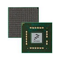
MPC8536DS Freescale Semiconductor, MPC8536DS Datasheet - Page 347

MPC8536DS
Manufacturer Part Number
MPC8536DS
Description
BOARD DEV SYSTEM MPC8536E
Manufacturer
Freescale Semiconductor
Series
PowerQUICC III™r
Type
MPUr
Datasheets
1.MPC8536EBVTAVLA.pdf
(127 pages)
2.MPC8536EBVTAVLA.pdf
(1706 pages)
3.MPC8536DS.pdf
(2 pages)
4.MPC8536DS.pdf
(126 pages)
Specifications of MPC8536DS
Contents
Board, Software and Documentation
Processor Series
MPC85xx
Core
e500
Data Bus Width
32 bit
Maximum Clock Frequency
667 MHz
Operating Supply Voltage
- 0.3 V to + 1.21 V
Maximum Operating Temperature
+ 105 C
Data Ram Size
32 KB
Interface Type
SPI, USB
Program Memory Type
DDR2, DDR3, SDRAM
Core Size
32 Bit
Program Memory Size
544KB
Cpu Speed
1.5GHz
Digital Ic Case Style
BGA
No. Of Pins
783
Supply Voltage Range
0.95V To 1.05V
Rohs Compliant
Yes
For Use With/related Products
MPC8536
Lead Free Status / RoHS Status
Lead free / RoHS Compliant
- MPC8536EBVTAVLA PDF datasheet
- MPC8536EBVTAVLA PDF datasheet #2
- MPC8536DS PDF datasheet #3
- MPC8536DS PDF datasheet #4
- Current page: 347 of 1706
- Download datasheet (15Mb)
Single-beat writes are performed by masking the last three (or seven) beats of the four- (or eight-) beat
burst using the data mask MDM[0:8]. If ECC is disabled, writes smaller than double words are performed
by appropriately activating the data mask. If ECC is enabled, the controller performs a read-modify write.
To accommodate available memory technologies across a wide spectrum of operating frequencies, the
DDR memory controller allows the setting of the intervals defined in
memory clock cycle, except for CASLAT, which can be programmed with 1/2 clock granularity.
Freescale Semiconductor
WR_DATA_DELAY
Timing Intervals
ACTTOPRE
ACTTOACT
PRETOACT
ACTTORW
BSTOPRE
WRTORD
REFREC
CASLAT
WRREC
REFINT
If a second read or write is pending, reads shorter than four beats are not
terminated early even if some data is irrelevant.
The number of clock cycles from a bank-activate command until another bank-activate command within
a physical bank. This interval is listed in the AC specifications of the SDRAM as t
The number of clock cycles from an activate command until a precharge command is allowed. This
interval is listed in the AC specifications of the SDRAM as t
The number of clock cycles from an activate command until a read or write command is allowed. This
interval is listed in the AC specifications of the SDRAM as t
The number of clock cycles to maintain a page open after an access. The page open duration counter
is reloaded with BSTOPRE each time the page is accessed (including page hits). When the counter
expires, the open page is closed with an SDRAM precharge bank command as soon as possible.
Used in conjunction with additive latency to obtain the READ latency. The number of clock cycles
between the registration of a READ command by the SDRAM and the availability of the first piece of
output data. If a READ command is registered at clock edge
data is available nominally coincident with clock edge
allowed. This interval is listed in the AC specifications of the SDRAM as t
Refresh interval. Represents the number of memory bus clock cycles between refresh cycles.
Depending on DDR_SDRAM_CFG_2[NUM_PR], some number of rows are refreshed in each SDRAM
bank during each refresh cycle. The value of REFINT depends on the specific SDRAMs used and the
frequency of the interface as t
be calculated by referring to the AC specification of the SDRAM device. The AC specification indicates
a maximum refresh-to-activate interval in nanoseconds.
Provides different options for the timing between a write command and the write data strobe. This allows
write data to be sent later than the nominal time to meet the SDRAM timing requirement between the
registration of a write command and the reception of a data strobe associated with the write command.
The specification dictates that the data strobe may not be received earlier than 75% of a cycle, or later
than 125% of a cycle, from the registration of a write command. This parameter is not defined in the
SDRAM specification. It is implementation-specific, defined for the DDR memory controller in
TIMING_CFG_2.
The number of clock cycles from the last beat of a write until a precharge command is allowed. This
interval, write recovery time, is listed in the AC specifications of the SDRAM as t
Last write pair to read command. Controls the number of clock cycles from the last write data pair to the
subsequent read command to the same bank as t
The number of clock cycles from a precharge command until an activate or a refresh command is
The number of clock cycles from the refresh command until an activate command is allowed. This can
MPC8536E PowerQUICC III Integrated Processor Reference Manual, Rev. 1
Table 8-62. DDR SDRAM Interface Timing Intervals
RP
.
NOTE
Definition
WTR
n
.
+
m
RAS
RCD
Table 8-62
n
.
, and the read latency is
.
.
RP
with granularity of one
.
WR
DDR Memory Controller
RRD
.
.
m
clocks, the
8-73
Related parts for MPC8536DS
Image
Part Number
Description
Manufacturer
Datasheet
Request
R
Part Number:
Description:
Manufacturer:
Freescale Semiconductor, Inc
Datasheet:
Part Number:
Description:
Manufacturer:
Freescale Semiconductor, Inc
Datasheet:
Part Number:
Description:
Manufacturer:
Freescale Semiconductor, Inc
Datasheet:
Part Number:
Description:
Manufacturer:
Freescale Semiconductor, Inc
Datasheet:
Part Number:
Description:
Manufacturer:
Freescale Semiconductor, Inc
Datasheet:
Part Number:
Description:
Manufacturer:
Freescale Semiconductor, Inc
Datasheet:
Part Number:
Description:
Manufacturer:
Freescale Semiconductor, Inc
Datasheet:
Part Number:
Description:
Manufacturer:
Freescale Semiconductor, Inc
Datasheet:
Part Number:
Description:
Manufacturer:
Freescale Semiconductor, Inc
Datasheet:
Part Number:
Description:
Manufacturer:
Freescale Semiconductor, Inc
Datasheet:
Part Number:
Description:
Manufacturer:
Freescale Semiconductor, Inc
Datasheet:
Part Number:
Description:
Manufacturer:
Freescale Semiconductor, Inc
Datasheet:
Part Number:
Description:
Manufacturer:
Freescale Semiconductor, Inc
Datasheet:
Part Number:
Description:
Manufacturer:
Freescale Semiconductor, Inc
Datasheet:
Part Number:
Description:
Manufacturer:
Freescale Semiconductor, Inc
Datasheet:


