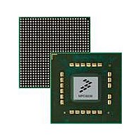
MPC8536DS Freescale Semiconductor, MPC8536DS Datasheet - Page 647

MPC8536DS
Manufacturer Part Number
MPC8536DS
Description
BOARD DEV SYSTEM MPC8536E
Manufacturer
Freescale Semiconductor
Series
PowerQUICC III™r
Type
MPUr
Datasheets
1.MPC8536EBVTAVLA.pdf
(127 pages)
2.MPC8536EBVTAVLA.pdf
(1706 pages)
3.MPC8536DS.pdf
(2 pages)
4.MPC8536DS.pdf
(126 pages)
Specifications of MPC8536DS
Contents
Board, Software and Documentation
Processor Series
MPC85xx
Core
e500
Data Bus Width
32 bit
Maximum Clock Frequency
667 MHz
Operating Supply Voltage
- 0.3 V to + 1.21 V
Maximum Operating Temperature
+ 105 C
Data Ram Size
32 KB
Interface Type
SPI, USB
Program Memory Type
DDR2, DDR3, SDRAM
Core Size
32 Bit
Program Memory Size
544KB
Cpu Speed
1.5GHz
Digital Ic Case Style
BGA
No. Of Pins
783
Supply Voltage Range
0.95V To 1.05V
Rohs Compliant
Yes
For Use With/related Products
MPC8536
Lead Free Status / RoHS Status
Lead free / RoHS Compliant
- MPC8536EBVTAVLA PDF datasheet
- MPC8536EBVTAVLA PDF datasheet #2
- MPC8536DS PDF datasheet #3
- MPC8536DS PDF datasheet #4
- Current page: 647 of 1706
- Download datasheet (15Mb)
Table 13-2
Freescale Semiconductor
Signal
LALE
LSYNC_OUT
MSRCID[0:4]
LSYNC_IN
LUPWAIT/
LAD[0:31]
LCLK[0:2]
LDP[0:3]
LA[7:31]
LGPL0/
LGPL1/
LGPL2/
LGPL3/
LGPL4/
MDVAL
LFCLE
LPBSE
LGPL5
LBCTL
LFALE
LFRB/
Name
LFWP
LGTA/
LFRE
LOE/
shows the detailed external signal descriptions for the eLBC.
I/O
O
Table 13-2. Enhanced Local Bus Controller Detailed Signal Descriptions
External address latch enable. The local bus memory controller provides control for an external address
latch, which allows address and data to be multiplexed on the device pins.
Meaning
MPC8536E PowerQUICC III Integrated Processor Reference Manual, Rev. 1
State
Function(s)
Alternate
LUPWAIT
LPBSE
LGPL0
LFCLE
LGPL1
LGPL2
LGPL3
LGPL4
LFALE
LFWP
LFRE
LFRB
LGTA
LOE
Table 13-1. Signal Properties—Summary (continued)
—
—
—
—
—
—
—
—
—
—
Asserted/Negated—LALE is asserted with the address at the beginning of each memory
controller transaction. The number of cycles for which it is asserted is governed by the
ORn[EAD] and LCRR[EADC] fields. Note that no other control signals are asserted
during the assertion of LALE.
eLBC debug
eLBC debug
GPCM
GPCM
Mode
UPM
UPM
UPM
UPM
UPM
UPM
UPM
FCM
FCM
FCM
FCM
FCM
—
—
—
—
—
—
—
—
General purpose line 0
Flash command latch enable
General purpose line 1
Flash address latch enable
Output enable
Flash read enable
General purpose line 2
General purpose line 3
Flash write protect
Transaction termination
Flash ready/busy, open-drain shared pin
General purpose line 4
External device wait
Local bus parity byte select
General purpose line 5
Data buffer control
Non-multiplexed address bus
Multiplexed address/data bus
Local bus data parity
Local bus clocks
PLL synchronize input
PLL synchronize output
Local bus data valid
Local bus source ID
Description
Descriptions
Enhanced Local Bus Controller
Signals
No. of
25
32
1
1
1
1
1
1
1
1
1
1
1
1
1
1
1
1
4
3
1
1
1
5
I/O
I/O
I/O
O
O
O
O
O
O
O
O
O
O
O
O
O
I
I
I
I
13-5
Related parts for MPC8536DS
Image
Part Number
Description
Manufacturer
Datasheet
Request
R
Part Number:
Description:
Manufacturer:
Freescale Semiconductor, Inc
Datasheet:
Part Number:
Description:
Manufacturer:
Freescale Semiconductor, Inc
Datasheet:
Part Number:
Description:
Manufacturer:
Freescale Semiconductor, Inc
Datasheet:
Part Number:
Description:
Manufacturer:
Freescale Semiconductor, Inc
Datasheet:
Part Number:
Description:
Manufacturer:
Freescale Semiconductor, Inc
Datasheet:
Part Number:
Description:
Manufacturer:
Freescale Semiconductor, Inc
Datasheet:
Part Number:
Description:
Manufacturer:
Freescale Semiconductor, Inc
Datasheet:
Part Number:
Description:
Manufacturer:
Freescale Semiconductor, Inc
Datasheet:
Part Number:
Description:
Manufacturer:
Freescale Semiconductor, Inc
Datasheet:
Part Number:
Description:
Manufacturer:
Freescale Semiconductor, Inc
Datasheet:
Part Number:
Description:
Manufacturer:
Freescale Semiconductor, Inc
Datasheet:
Part Number:
Description:
Manufacturer:
Freescale Semiconductor, Inc
Datasheet:
Part Number:
Description:
Manufacturer:
Freescale Semiconductor, Inc
Datasheet:
Part Number:
Description:
Manufacturer:
Freescale Semiconductor, Inc
Datasheet:
Part Number:
Description:
Manufacturer:
Freescale Semiconductor, Inc
Datasheet:


